This blog contains short questions and answers for AKTU Electronic Engineering students. Topics covered include semiconductor diodes, diode applications, BJT and FET, operational amplifiers, and electronic instrumentation, providing students with a thorough review of key topics and preparing them for tests.
Dudes 🤔.. You want more useful details regarding this subject. Please keep in mind this as well.

Important Questions For Electronic Engineering:
*Unit-01     *Unit-02
*Unit-03    *Unit-04
*Unit-05    *Short-Q/Ans
*Question-Paper with solution 21-22
Unit 1 Semiconductor Diode | Important Short Questions Answer
Q1. Why Si is preferred over Ge for manufacturing of electronics devices?
Ans. Si is preferred over Ge for manufacturing of electronic devices due to following reasons :
- i. The earth’s surface has an abundant supply of silicon. Manufacturers of semiconductor devices employ silicon primarily for this reason.
- ii. Cheaper.
- iii. Smaller leakage current.
- iv. Suitable for low power and high power applications.
Q2. Explain the effect of temperature on conductivity of a semiconductor.
Ans. A large number of covalent bonds will be broken and a large number of electrons and holes will be produced when the temperature rises in an intrinsic semiconductor, which will result in a smaller reduction in conductivity and an increase in conductivity of a large value.
Q3. Distinguish between avalanche and zener breakdown.
Ans.
| S. No. | Zener breakdown mechanism | Avalanche breakdown mechanism |
| 1. | The location of this breakdown mechanism is an extremely thin junction. | This breakdown process takes place in a somewhat thick junction. |
| 2. | Zener current is independent of applied voltage. | Avalanche breakdown occurs at high voltages. |
| 3. | Temperature coefficient is negative i .e. , -1.4 mV/°C. | Temperature coefficient is positive i.e., 2m V/°C . |
Q4. Differentiate between Transition capacitance (CT) and Diffusion capacitance ( CD)of a p-n junction diode.
Ans.
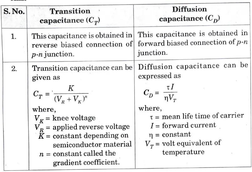
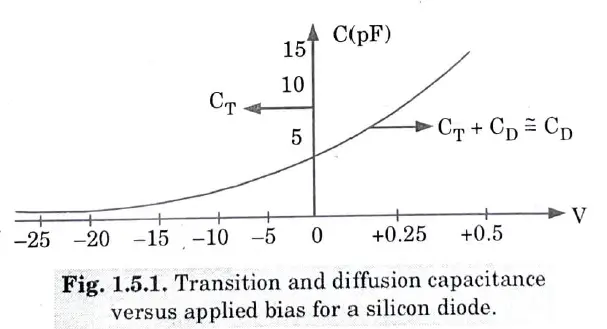
Q5. Draw the characteristics of transition – and diffusion capacitance v/s applied bias voltage.
Ans.
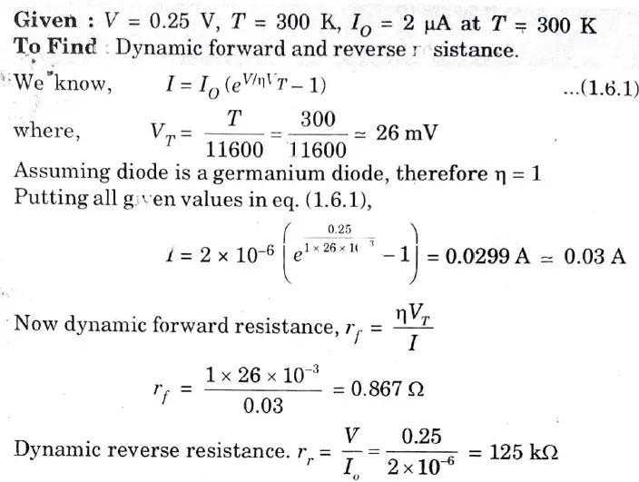
Q6. Calculate the dynamic forward and reverse resistance of a p -n j unction diode when the applied voltage is 0.25 V at T=300 K given lO =2μA.
Ans.
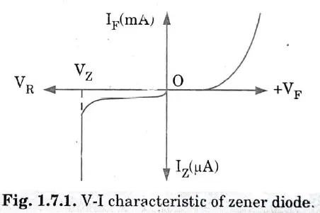
Q7. Draw the V-1 characteristic of a zener diode regulates the voltages.
Ans.
Q8. Compare the properties of Si and Ge Semiconductors.
Ans.
| S. No. | Properties | Si | Ge |
| 1. | Conductivity. | Comparatively low. | Conductivity is comparatively higher. |
| 2. | Atomic radius. | Has a smaller atomic radius than germanium. | Has comparatively a larger atomic radius. |
Q9. Define depletion layer in a diode. OR Define depletion layer of PN junction diode.
Ans. Due to the “depletion” of free carriers in the region, the zone of exposed positive and negative ions is known as the depletion region.
Q10. Define bulk resistance of the diode.
Ans. How a diode is biassed affects its bulk resistance. It represents the estimated resistance of a forward biassed diode.
Q11. Classify the materials with help of energy band.
Ans. On the basis of .energy band diagram, materials are classified into three types :
1. Insulators :The valence band is full while the conduction band is empty in insulators. Valence and conduction bands have a very wide energy gap.
2. Conductors : The valence and conduction bands overlap in the case of conductors.
3. Semiconductors : In semiconductors, the valence band is nearly full, the conduction band is nearly empty, and there is a very small energy gap between the two bands.
Unit 2 Diode Applications | Short Questions With Answer
Q1. Draw a neat diagram of a full wave rectifier bridge circuit using diode.
Ans.
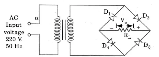
Q2. What are the PIV for full wave center tapped rectifier and bridge rectifier respectively?
Ans. In center tap full wave rectifier, PIV = 2 Vm
In bridge type full wave rectifier, PIV = Vm
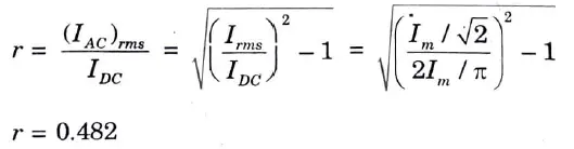
Q3. What is the ripple factor for full wave rectifier ?
Ans.
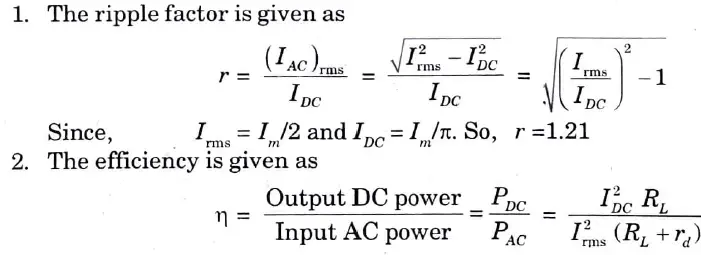
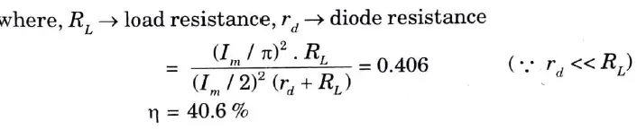
Q4. Write an expression for the ripple factor and efficiency for half wave rectifier.
Ans.
Q5. What is the voltage multiplier ?
Ans. Voltage-multiplier circuits are used to boost the peak output voltage to two, three, four, or more times the peak rectified voltage while maintaining a relatively low transformer peak voltage.
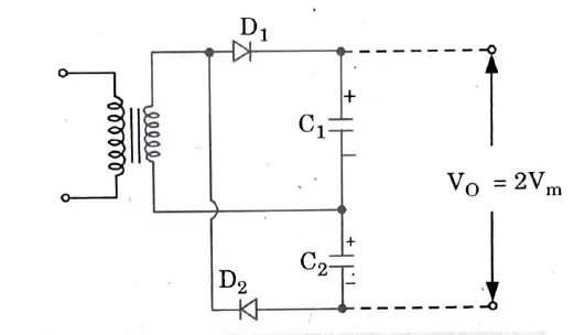
Q6. Draw the circuit diagram of full wave voltage doubler using diode.
Ans.
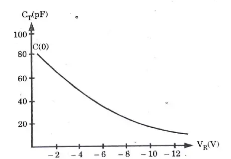
Q7. Draw the capacitance versus voltage transfer characteristics for the Varactor Diode.
Ans.
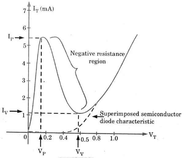
Q8. Draw V-I characteristics of a Tunnel Diode.
Ans.
Q9. What will happen to the number of free electrons in a semiconductor on increasing temperature ?
Ans. The doped portions of a semiconductor experience more free electrons and holes as the temperature rises. Therefore, as the temperature rises, there are more free electrons.
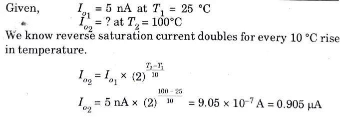
Q10. A silicon diode has a saturation current of 5 nA at 25 °C. What is the saturation current at 100 °C ?
Ans.
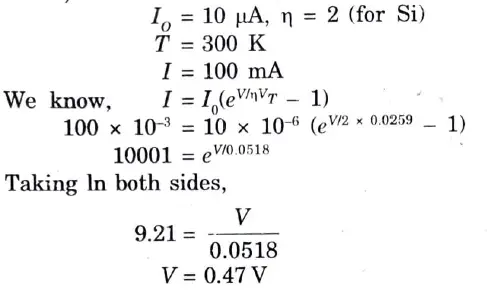
Q11. The reverse saturation current of a silicon p-n junction diode is 10 μA at the temperature 300 K. Determine the forward bias voltage to be applied across the p-n junction to obtain a current of around 100 mA.
Ans. Given
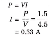
Q12. A 4.5 V zener is rated at 1.5 watt. What is the maximum safe – current of the zener ?
Ans.
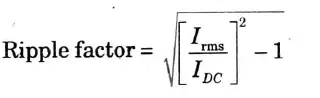
Q13. What is ripple factor?
Ans. Ripple factor: The ratio of the peak value of the output’s AC component to its average or DC component is known as the ripple factor. It is given by,
Q14. Explain the principle of operation of LED.
Ans. i. Generation of electron – hole pair (EHP) by excitation of semiconductor.
ii. Recombination of EHP.
iii. Extraction of photons from the semiconductor.
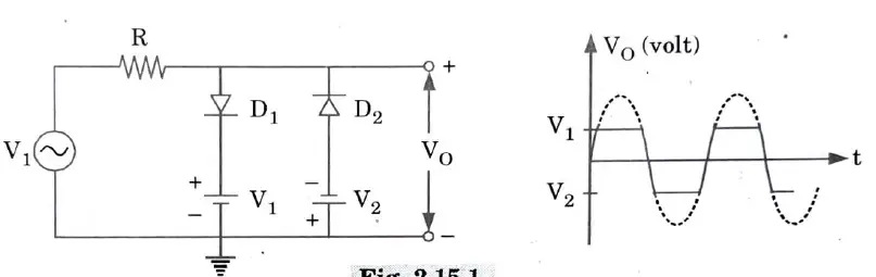
Q15. Draw the double ended diode clipper circuit.
Ans.
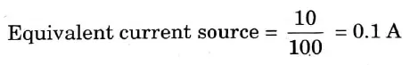
Q16. Consider a constant voltage source }Vith 10 V and series internal resistance of 100 ohm. Calculate its equivalent to a current source.
Ans.
Unit 3 BJT and FET | AKTU Short Question for Exam
Q1. What are the various operating modes of transistor ?
Ans. There are 4 different modes of transistor :
| S. No. | Mode | BE | CB |
| 1. | Active | Forward bias | Reverse bias |
| 2. | Saturation | Forward bias | Forward bias |
| 3. | Cut-off | Reverse bias | Reverse bias |
| 4. | Inverse active | Reverse bias | Forward bias |
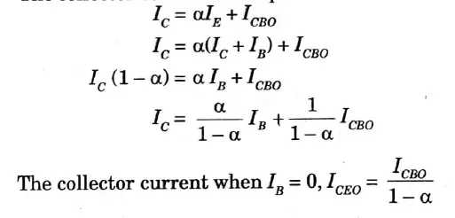
Q2. Establish the relationship between lCEO and lCBO of a BJT.
Ans. The collector current can expressed as
Q3. What is major difference between a bipolar and unipolar device?
Ans.
| S. No. | Bipolar device | Unipolar device |
| 1. | It has low input impedance. | It has high input resistance inorder of 100 MΩ i.e., high. |
| 2. | It is more noisy. | It is less noisy. |
| 3. | It is more affected by radiation. | Radiation affects less. |
| 4. | Cost is less. | Cost is high. |
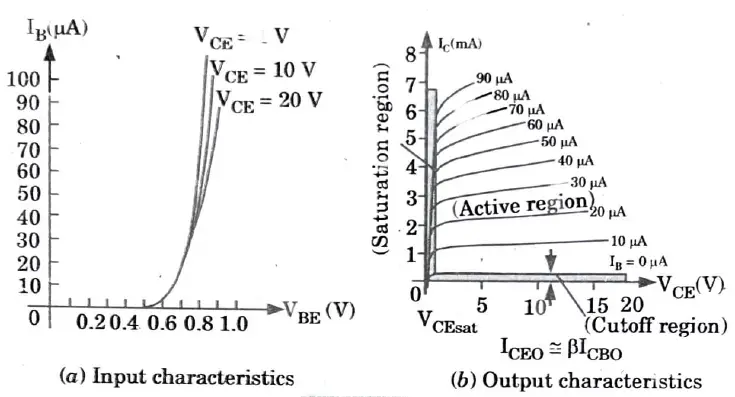
Q4. Sketch the input and output characteristics (V-1) of a CE npn transistor configuration with proper labels.
Ans.
Q5. Enlist. the difference between JFET and BJT.
Ans.
| S.No. | JFET | BJT |
| 1. | It is a unipolar device since it only operates with carriers in the majority. | It is a bipolar device since its operation is dependent on both majority and minority carriers. |
| 2. | It is a voltage controlled device. | It is a current controlled device. |
| 3. | It has high input impedance. | It has low input impedance. |
| 4. | Small size means that there isn’t much space needed on board. | Large size necessitates a large amount of space on board. |
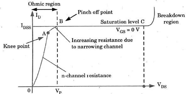
Q6. Draw the transfer and output characteristics of n-channel FET.
Ans. A Transfer characteristics :
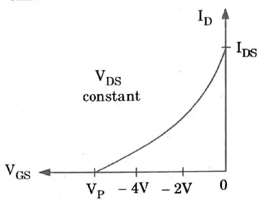
B. Output characteristics :
Q7. Enlist the differences between JFET and MOSFET.
Ans.
| S. No. | JFET | MOSFET |
| 1. | Compared to MOSFET, JFETs have a lower input resistance. | Compared to JFET, MOSFET has a substantially higher input resistance. |
| 2. | JFET can operate in depletion mode. | Both enhancement and depletion modes of operation are possible for MOSFET. |
Q8. Write down the constructional difference between depletion type and enhancement type MOSFET.
Ans. The main constructional difference is the absence of continuous channel between the source and drain of enhancement MOSFET but it is present in case of depletion MOSFET.
Q9. Mention the differences between-channel and n-channel MOSFET.
Ans.
| S. No. | p-channel MOSFET | n-channel MOSFET |
| 1. | The current carriers are holes. | The current carriers areelectrons. |
| 2. | P-channel has lower transconductance than n-channel. | Compared to p-channel, n-channel has greater transconductance. |
| 3. | P-channel is slower than n-channel because holes are less mobile. | N-channel MOSFETs operate more quickly because electron mobility is higher. |
Q10. Describe how FET can used as voltage variable resistor.
Ans. FET when used in the region before pinch-off, it works as variable resistance device i.e., the channel resistance is controlled by the gate bias voltage (VGS).In such applications FET is referred as voltage variable resistor (VVR).
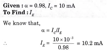
Q11. The BJT circuitry has Ic = 10 mA and a=· 0.98. Determine the value of IE.
Ans.
Q12. Why BJT is called current controlled device ?
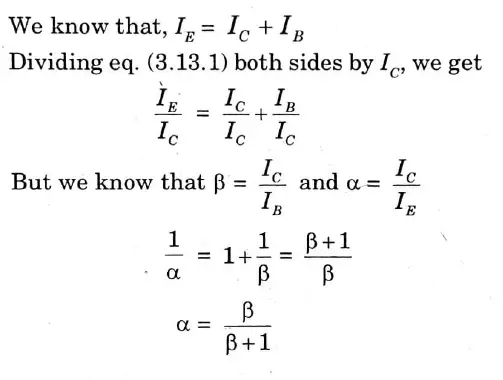
Ans. Because the base current controls the current flow from the emitter to the collector, a BJT is referred to as a current control device.Q13. Derive the relation between α and β for BJT.
Q13. Derive the relation between α and β for BJT.
Ans.
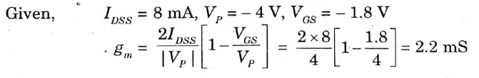
Q14. In JFET, IDSS =_8 mA, VP = – 4 V biased at VGS = – 1.8 V. Determine the value of gm·
Ans.
Q15. Define Ohmic region in FET.
Ans. 1. FETs function as linear, or resistor-like, devices in the ohmic zone. Voltage-variable resistors (VVR) and voltage dependent resistors are two examples (VDR).
2. In the ohmic region, FET will work as a voltage-variable resistor by varying VGS·
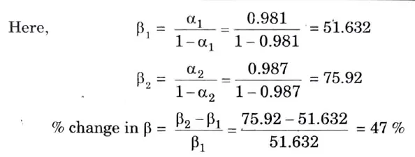
Q16. If α of a transistor changes from 0.981 to 0.987, find the percentage change in β.
Ans.
Q17. The thickness of base is typically smaller than emitter and collector. Why?
Ans. In order to send the majority of the injected charge carriers to the collector, the base is both extremely heavily doped and thin (l0–6 m) in comparison to either the emitter or the collector.
Q18. Why are FET called unipolar device ?
Ans. FETs are unipolar devices because current conduction in them only depends on one type of carrier (majority carriers), either electrons or holes.
Q19. Explain with proper reason the use of Emitter Follower.
Ans. A high resistance source is connected to a low resistance load using an emitter follower as a voltage buffer.
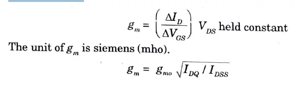
Q20. What is trans-conductance in FET? What is the relationship between gm and gmo?
Ans. The control that the gate voltage has over drain current is measured by transconductance gm. It is simply the slope of transfer characteristics.
Unit 4 Operational Amplifier | Important AKTU Questions
Q1. Write the characteristics of an ideal op-amp.
Ans.
- 1. Input impedance is infinite.
- 2. Output impedance is zero.
- 3. Infinite CMRR.
- 4. Bandwidth is infinite.
- 5. Open loop gain is infinite.
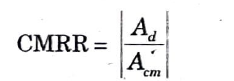
Q2. Define CMMR, slew rate of Op-Amp.
Ans. 1. CMRR : The common mode rejection ratio (CMRR) of a differential amplifier describes its capacity to reject a common mode signal. CMRR is defined as the ratio of the differential voltage gain Ad to the common mode voltage gainAcm i.e.,
2. Slew rate (SR) : It is defined as the maximum rate of change of output voltage per unit time and is expressed in volts per microsecond i.e.,
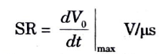
Slew rate describes how quickly an Op-output Amp’s can change in response to an input frequency change
Q3. What do you understand by single-ended and double-ended operations of Op-Amp ?
Ans. The operation is referred to as single-ended if an input signal is applied to either input while the other input is grounded. The operation is referred to as double ended if two input signals of opposite polarity are applied.
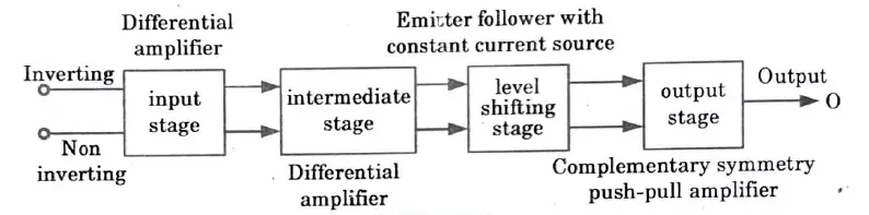
Q4. Define Op-Amp and draw its block diagram.
Ans. Op-Amp : The purpose of an operational amplifier is to carry out different mathematical operations, including addition, subtraction, integration, differentiation, etc.
Block diagram :
Q5. Define cut off frequency and give the relation between unity gain frequency and cut off frequency.
Ans. Cut off frequency is defined as the frequency at which the gain
drops by 3 db (or to 0 .707 the DC gain,Avd) and it is denoted by fc. Relation between unity gain frequency (f1) and cut off frequency (fc) is given by
f1 = Avd fc
where Avd = Voltage differential gain or DC gain.
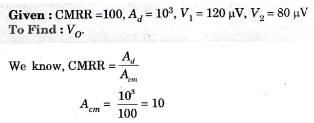
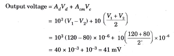
Q6 An operational amplifier has a differential gain of 103 and a CMRR of 100, input voltages are 120 μV and 80 μV. Determine the output voltage.
Ans.
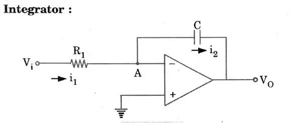
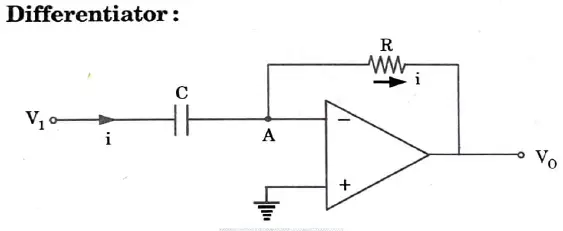
Q7. Sketch the circuit of op-amp as an integrator and differentiator.
Ans.
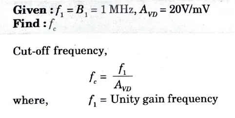
Q8. Determine the cut-off frequency of an Op-Amp having specified value B1 = 1 MHz and Avn = 20 V/mV.
Ans.

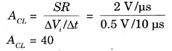
Q9. For an Op-Amp having a slew rate of SR= 2 V/μs, what is the maximum closed loop voltage gain that can be used when ·the input varies by 0.5 V in 10 μs ?
Ans. Closed loop gain,
Q10. How voltage follower is used for impedance matching applications ?
Ans. A voltage follower has an extremely low output impedance and a very high input impedance of the order of MΩ. As a result, this circuit uses very little source current. In impedance matching applications, the voltage follower can therefore be utilised as a buffer between a high impedance source and a low impedance load.
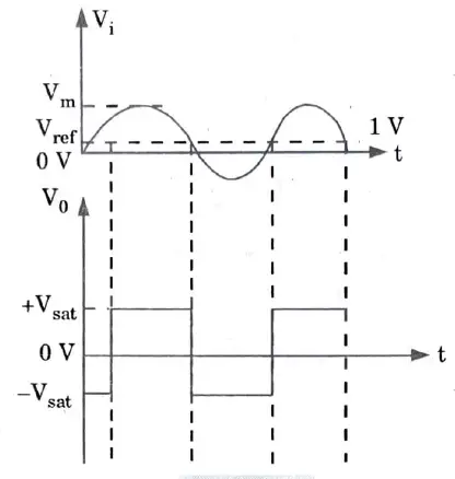
Q11. Draw the output waveform that will appear across RL.
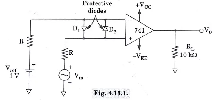
Ans.
Unit – 5 Electronics Instrumentation and Measurements
Q1. Define digital voltmeter. Give its classifications.
Ans. DVM : The digital voltmeter (DVM) is a tool for indication. DVM’s primary application is for measuring voltage between two locations. It shows discrete numerals for either DC or AC voltage.
Classification :
- i. Non-integrating DVM
- ii. Integrating DVM
Q2. What is multimeter and write its applications ?
Ans. Multimeter : A measuring device that combines multiple measurement operations into a single electronic device.
Applications : Used to measure :
- i. AC / DC voltage
- ii. AC / DC current
- iii. Resistance
Q3. Define the. horizontal and vertical sensitivity of a CRT.
Ans. Horizontal sensitivity: The horizontal deflecting voltage will determine how much of a horizontal deflection (x) is created, Vx, applied to x-input.
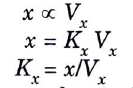
where Kx expressed as cm/volt or division/volt, is called horizontal sensitivity of CRT.
Vertical sensitivity : The vertical deflection (y) produced will be proportional to the vertical deflecting voltage, V y, applied to the y-input.
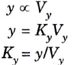
where KY expressed as cm/volt or division/volt is called vertical sensitivity of CRT.
Q4. What are the functions of a delay line and trigger circuit ?
Ans. In order to synchronize the input signal and the sweep frequency, the input signal is delayed in the vertical section of the device using a delay line, while the trigger circuit converts the delayed signal into trigger pulses.
Q5. What is CRO ?
Ans. The cathode ray oscilloscope is a very useful and adaptable laboratory tool for measuring voltage, current, power, and frequency as well as for examining the waveforms of alternating currents and voltages.
Q6. State the advantage of digital instruments over analog instruments.
Ans.
- i. Greater accuracy
- ii. Better resolution and easy readability
- iii. High input resistance.
Q7. A digital voltmeter has negligible loading effect on the circuit under test. Why ?
Ans. Due to their extremely high input resistance, digital voltmeters have a very small loading effect on the circuit being tested.
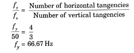
Q8. A Lissajous pattern on an oscilloscope is stationary and has 4 horizontal and 3 vertical tangencies. The horizontal frequency is 50 Hz, find vertical frequency.
Ans.
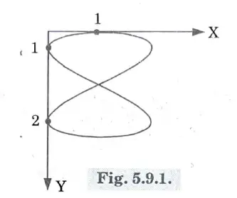
Q9. Draw the Lissajous pattern w hen the ratio of the frequency of the vertical input to that o f horizontal input is 1 : 2.
Ans.
Q10. List the four specifications of unregulated power supply.
Ans.
- i. Current application
- ii. Output voltage
- iii. Output ripple
- iv. Load regulation

Electronic Engineering Quantum PDF, Syllabus, Important Questions
| Label | Link |
|---|---|
| Subject Syllabus | Syllabus |
| Short Questions | Short-question |
| Important Unit-1 | Unit-1 |
| Important Unit-2 | Unit-2 |
| Important Unit-3 | Unit-3 |
| Important Unit-4 | Unit-4 |
| Important Unit-5 | Unit-5 |
| Question paper – 2021-22 | 2021-22 |
Electronic Engineering Quantum PDF | AKTU Quantum PDF:
| Quantum Series | Links |
| Quantum -2022-23 | 2022-23 |
AKTU Important Links | Btech Syllabus
| Link Name | Links |
|---|---|
| Btech AKTU Circulars | Links |
| Btech AKTU Syllabus | Links |
| Btech AKTU Student Dashboard | Student Dashboard |
| AKTU RESULT (One VIew) | Student Result |