Prepare yourself for your Electronic Engineering exams with crucial questions and answers from Unit 1: Semiconductor Diodes for AKTU students. For evaluate success, improve your knowledge of diode characteristics, rectifiers, and other topics.
Dudes 🤔.. You want more useful details regarding this subject. Please keep in mind this as well.

Important Questions For Electronic Engineering:
*Unit-01     *Unit-02
*Unit-03    *Unit-04
*Unit-05    *Short-Q/Ans
*Question-Paper with solution 21-22
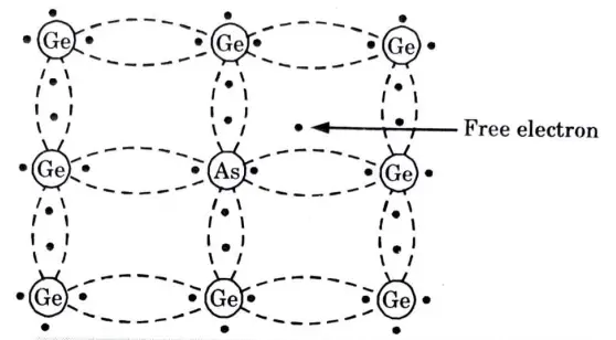
Q1. Explain n-type and p-type semiconductors.
Ans. i. n-type Semiconductor :
- 1. The resulting crystal is known as an n-type extrinsic semiconductor when a little quantity of pentavalent impurity is added to a pure semiconductor crystal during the crystal formation process.
- 2. In the figure, arsenic (As) is introduced to a germanium (Ge) crystal in such a way that four of the latter’s valence electrons establish a covalent link with the other four.
- 3. The fifth electron in arsenic is a free electron since it is not bound.
- 4. This electron is a potential current carrier. With every other semiconductor, this free electron serves as a donor whenever necessary.
- 5. The electrons are the majority carriers while holes are the minority carriers in such cases.
ii. p-type Semiconductor:
- 1. The crystal that results when a tiny amount of trivalent impurity is added to pure crystal during crystal formation is known as a p-type extrinsic semiconductor.
- 2. Fig. shows each atom of boron i.e., trivalent impurity is added to pure germanium crystal.
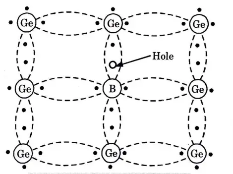
- 3. Three valence electrons form a covalent bond, a fourth covalent bond is created by the contribution of the germanium atom, and a hole results from the absence of one electron.
- 4. The fourth electron that is left seeks to create a bond as well and is referred to as the acceptor.
- 5. The majority carriers in a p-type semiconductor are holes, while the minority carriers are electrons.
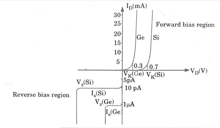
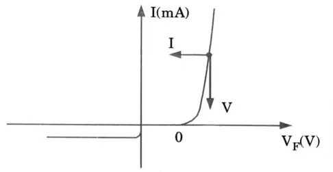
Q2. Explain the V-1 characteristic of p-n junction diode. Draw well labelled characteristic.
Ans. i. Forward bias :
- 1. P-type is connected to the positive terminal of the battery while then-type is connected to the negative terminal for the forward bias of a p-n junction.
- 2. With a potential divider, the potential can be changed. The potential barrier is removed and current flow begins at a certain forward voltage (0.3 V for Ge and 0. 7 V for Si). This voltage is also referred to as the knee voltage (VK).
- 3. The forward current increases exponentially when the forward voltage applied rises above the threshold voltage, as seen in Fig.
- 4. Beyond a certain safe value, it generates an incredibly high current that could cause the junction to overheat and fail.
ii. Reverse bias :
- 1. The positive terminal of a battery is connected to an n-type whereas the negative terminal is attached to a p-type.
- 2. In this situation, the junction resistance rises dramatically and the circuit’s current is essentially nonexistent.
- 3. Minority carriers cause a little current on the order of p.A to actually flow in the circuit. Reverse current is the term for this. In Fig., the reverse current is depicted.
- 4. The reverse current swiftly increases to its maximum or saturation value as the reverse bias is raised from zero. The tiny rise is caused by surface contaminants, which act as a resistor and hence follow Ohm’s law. A current known as surface leakage current results from this.
- 5. If the reverse voltage is raised even further, the electrons’ kinetic energy will be so high that they will knock out from semiconductor atoms. At this point, the junction breaks down, and the reverse current suddenly increases. The junction is now totally demolished.
- 6. Therefore, a p-n junction diode is a one-way device that acts like an insulator when reverse biassed and delivers low resistance when forward biassed. The ability to rectify, or change alternating current into direct current, makes it a useful device.
Comparison of V-1 characteristice of silicon and germanium diode:
- 1. The knee voltage for germanium and silicon diodes is 0.3 and 0.7 volts, respectively.
- 2. The breakdown voltage for silicon diode is greater than germanium diode.
- 3. In comparison to silicon diodes of equivalent ratings, the reverse saturation current in germanium diodes is 1,000 times higher.
Q3. Explain the resistance of a semiconductor diode and derive the expression for diode resistance.
Ans. Resistance of diode is,
i. DC or static resistance (RD):
- 1. DC resistance is defined as the voltage to current ratio in the p-n junction diode’s forward bias characteristics.
- 2. In general, higher the current through a diode, the lower is the DC resistance level.
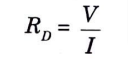
- 3. Using the appropriate values of voltage V and current I, the DC resistance at the operating point is calculated.
- 4. The shape of the characteristics in the area around the location of interest has no bearing on the DC resistance.
ii. AC or dynamic resistance (rd) :
- 1. The reciprocal of the slope of a diode’s V-I characteristics is known as AC resistance.
- 2. It is determined as
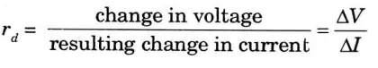
- 3. A straight line drawn perpendicular to the curve through the Q-point in the diode’s forward characteristics can be used to calculate AC resistance.
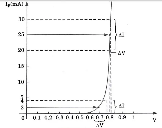
- 4. Higher AC resistance results from a lower Q-point of operation (smaller current or lower voltage).
- 5. The Shockley’s equation for the forward and r even:e bias is given by
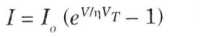
- 6. We are aware that the slope of the tangent line drawn at a given location is equal to the derivative of a function at that point.
- 7. Taking derivative of eq. with respect to applied voltage V, we get
- 8. AC resistance is the sum of ohmic resistance of the p and n type semiconductor and junction resistance, r j.

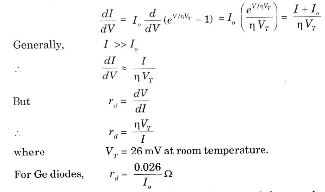
Iii. Average AC resistance (rav) : If the input signal is large enough to provide a variety of characteristics, it is the resistance connected to the AV device for the area.
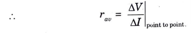
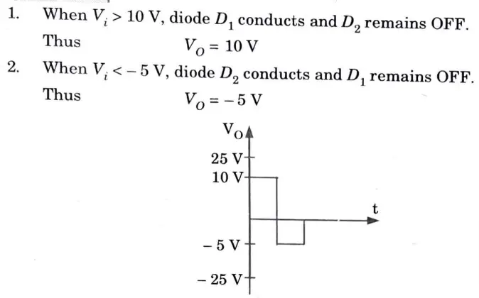
Q4. Sketch output voltage (VO) for the network of Fig. for the input given. Assume diodes are ideal.
Ans.
Q5. Explain the transition and diffusion capacitance.
Ans. i. Space charge o:t transition capacitance (CT):
- 1. The depletion region functions as an insulator in a reversed biassed p-n junction, while the low resistance p and n-type regions on either side serve as the plate.
- 2. In this way p-n junction may be regarded as parallel plate capacitor.
- 3. The junction capacitance is called space charge capacitance or transition capacitance and is denoted by CT.
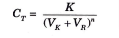
where VK= Knee voltage
VR = Applied reverse voltage
K = Constant depending on semiconductor material
n = (1/2) for alloy and (1/3) for diffusion junction.
- 4. Fig. shows the variation of transition capacitance with applied reverse voltage.
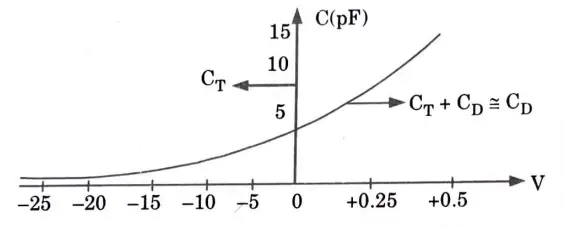
- 5. The transition capacitance (CT) are,
- a. With no applied voltage : CT= 20 pF
- b. With forward bias : CT = 25 pF
- c. With reverse bias : CT= 8pF
ii. Diffusion or storage capacitance (CD):
- 1. The potential barrier is lowered in a forward biassed p-n junction. Now, holes from the p-side enter into the n-side, and electrons from the n-side enter into the p-side.
- 2. These carriers gradually recombine as they disperse away from the junction. When a forward bias voltage is provided, a charge is subsequently stored on both sides of the junction.
- 3. As with a real capacitor, the amount of stored charge fluctuates with the applied potential.
- 4. The diffusion capacitance expressed by the equation CD= dQ/dV, where dQ represents the change in minority carriers stored outside the depletion region when a change in voltage across diode, dV, is applied.
- 5. The diffusion capacitance can be expressed as :
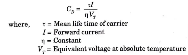
- 6. The value of CD is large for forward current and small for reverse current. Large value of CD delays both the switch-ON and switch-OFF.
Q6. Explain reverse breakdown of a diode.
Ans. Zener breakdown and avalanche breakdown are the two ways by which reverse breakdown can happen.
Zener breakdown :
- 1. It occurs in a very thin junction (i.e., depletion layer is narrow due to heavily doped junctions on both sides).
- 2. A very strong electric field (about 107 V/m) is created across the thin depletion layer when a tiny reverse bias voltage is applied.
- 3. The covalent bonds can be broken by this field alone. The reverse saturation current is made up of a lot of electrons and holes produced by this breakdown of covalent bonds (i.e., zener current).
- 4. The applied voltage has no effect on the zener current. Only the external resistance influences it.
- 5. This breakdown is called as zener breakdown as shown in Fig. This breakdown occurs at low voltage.
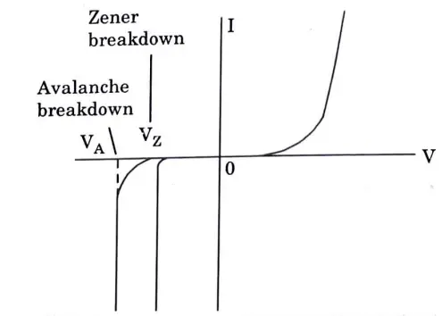
Avalanche breakdown :
- 1. When the connection is somewhat thicker than the case, avalanche breakdown occurs. It indicates that the junction’s two sides are mildly doped.
- 2. For the identical applied voltage of the breakdown case, the electric field across the depletion zone (layer) in this instance is not sufficiently enough to cause zener failure.
- 3. Here, the semiconductor atoms in the depletion region are struck by the minority carriers that have been accelerated by the field.
- 4. The kinetic energy of the electrons involved in a collision is transmitted covalently to other bonds, increasing the pair energy and leading to the covalent bonds being broken and the generation of electron-holes.
- 5. Due to the cumulative process of avalanche multiplication, the newly produced carriers transfer bonds and their energy to other covalent are generated break more bonds, leading to extraordinarily huge numbers of carriers.
- 6. This division At higher voltages, this breakdown, known as avalanche breakdown, as depicted in Fig., takes place.

Electronic Engineering Quantum PDF, Syllabus, Important Questions
| Label | Link |
|---|---|
| Subject Syllabus | Syllabus |
| Short Questions | Short-question |
| Important Unit-1 | Unit-1 |
| Important Unit-2 | Unit-2 |
| Important Unit-3 | Unit-3 |
| Important Unit-4 | Unit-4 |
| Important Unit-5 | Unit-5 |
| Question paper – 2021-22 | 2021-22 |
Electronic Engineering Quantum PDF | AKTU Quantum PDF:
| Quantum Series | Links |
| Quantum -2022-23 | 2022-23 |
AKTU Important Links | Btech Syllabus
| Link Name | Links |
|---|---|
| Btech AKTU Circulars | Links |
| Btech AKTU Syllabus | Links |
| Btech AKTU Student Dashboard | Student Dashboard |
| AKTU RESULT (One VIew) | Student Result |
6 thoughts on “Unit-1 Semiconductor Diodes, Electronic Engineering Qs & Solutions AKTU”