
This blog contains critical questions and answers for UNIT-3: BJT AND FET Electronic Engineering AKTU students. It discusses transistor biasing, amplifier designs, and other issues.
Dudes 🤔.. You want more useful details regarding this subject. Please keep in mind this as well.

Important Questions For Electronic Engineering:
*Unit-01     *Unit-02
*Unit-03    *Unit-04
*Unit-05    *Short-Q/Ans
*Question-Paper with solution 21-22
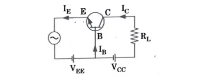
Q1. Draw the basic structure of CB BJT and explain its principle of operation with in neat diagram along with its input and output characteristics.
Ans. Common-base (CB) configuration :
1. The input signal is applied between the base and the emitter in this setup. As depicted in Fig., the output is gathered from the collector and base.
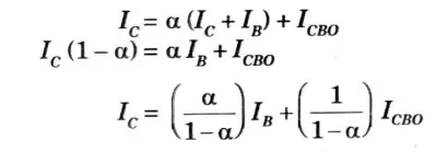
Current amplification factor (𝞪) :
1. It is defined as the ratio of the collector current t.o the emitter current of a transistor when no signal is applied and is called DC alpha (𝞪DC).
3. In the sense that collector current approaches emitter current, a transistor with a higher value is better.
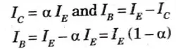
4. The current amplification factor is now defined as the ratio of change in collector to emitter current at constant collector base voltage when a signal is supplied.
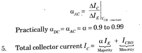
6. The collector current can also be expressed as
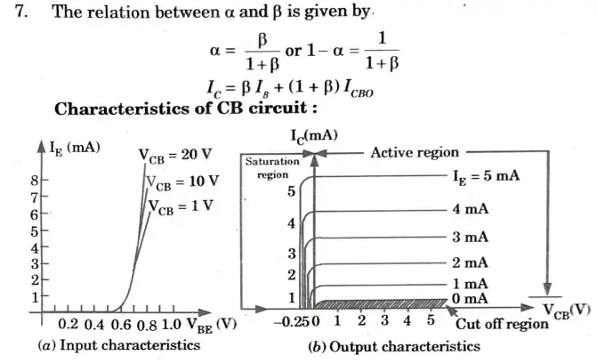
Input characteristics :
- i. There exists a cut in, offset or threshold voltage VBE below which the current is very small.
- ii. IE increases rapidly with small increase in VBE i.e., input resistance is very small.
Output characteristics :
- i. In active region, the collector current is independent of collector voltage and depends upon emitter current but if VCB increases beyond a certain value, IC increases rapidly due to avalanche breakdown. In this region, the base emitter function is forward biased whereas collector base function is reversed biased.
- ii. In cut off region, a small amount of collector current flows even when IE= 0. i.e., leakage current lCBO.
- Here emitter base and collector base junctions both are reversed biased
- iii. In saturation region, current IC flows even if VCB ≅ 0.
- Here collector and emitter junctions both are forward biased .
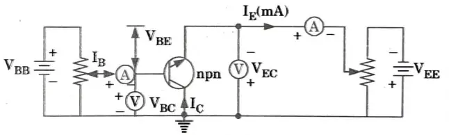
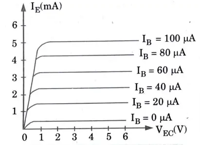
Q2. Explain the operation of common collector configuration with suitable characteristics in detail.
Ans. 1. Figure 1 depicts the circuit diagram for identifying a npn transistor’s static properties in the common collector arrangement.
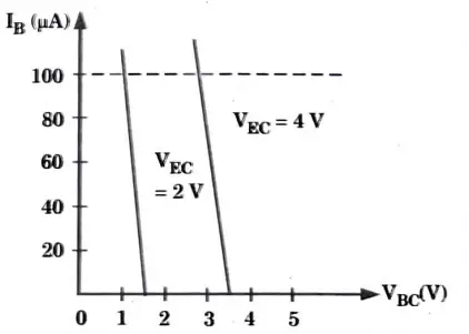
Input characteristics :
- 1. To determine the input characteristics, VEC is kept at a suitable fixed value.
- 2. The base-collector voltage VBC is increased in equal steps and the corresponding increase in IB is noted.
- 3. This is repeated for different fixed values of VEC Plot of VBC versus IB for different values of VEC is shown in Fig.
Output characteristics : 1. The output characteristics is shown in Fig. are the plots of VEC versus lC for different values of lB.
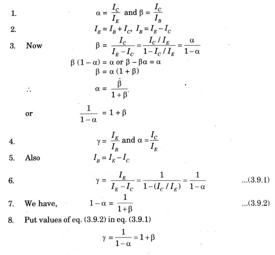
Q3. Derive the relation between 𝞪, 𝛃 and 𝞬.
Ans.
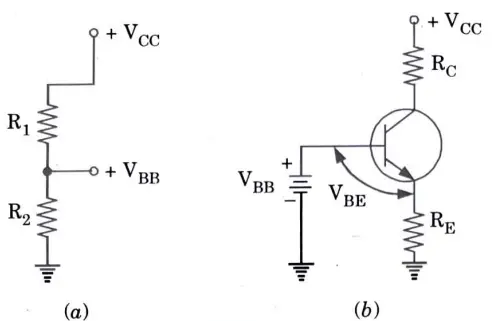
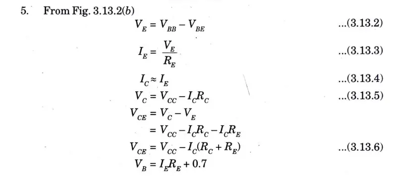
Q4. Explain the operation of voltage divider bias circuit and write down the approximate equations of VB , IE, IC and VCE.
Ans. Voltage Divider Bias :
1. Fig. shows the most widely used biasing circuit in this method, the base circuit contains a voltage divider (R1 and R2). Because of this, the circuit is called voltage divider bias (VDB).
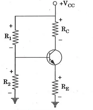
Circuit· analysis :
- 1. The base current in a VDB circuit is significantly less than the current flowing through the voltage divider.
- 2. So that we can obtain the equivalent circuit of Figure, we can open the connection between the voltage divider and the base.
- 3. In this circuit the output of the voltage divider is
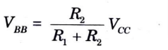
- 4. Ideally, this is the base-supply voltage as shown in Fig.
Q5. Explain how the input impedance of an amplifier can load down the AC source.
Ans. 1. The internal resistance of the voltage source is finite in practise. The input impedance of an amplifier can load down the AC source, that is, lower the AC voltage that appears across the emitter diode, if this internal resistance is taken into account in the amplifier’s AC analysis.
2. For a CE amplifier shown in the Fig.
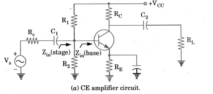
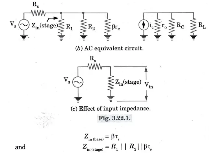
3. The AC source has to drive the input impedance of the stage Zin (stage).4. This input impedance includes the effects of the biasing resistors R1 and R2 in parallel with the input impedance of the base Zin (base).
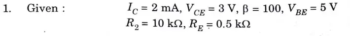
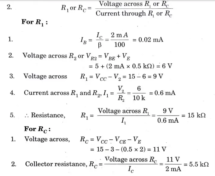
Q6. In the circuit shown in Fig. if lC = 2 mA and VCE= 3 V, calculate R1 and RC·
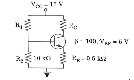
Ans.

Electronic Engineering Quantum PDF, Syllabus, Important Questions
| Label | Link |
|---|---|
| Subject Syllabus | Syllabus |
| Short Questions | Short-question |
| Important Unit-1 | Unit-1 |
| Important Unit-2 | Unit-2 |
| Important Unit-3 | Unit-3 |
| Important Unit-4 | Unit-4 |
| Important Unit-5 | Unit-5 |
| Question paper – 2021-22 | 2021-22 |
Electronic Engineering Quantum PDF | AKTU Quantum PDF:
| Quantum Series | Links |
| Quantum -2022-23 | 2022-23 |
AKTU Important Links | Btech Syllabus
| Link Name | Links |
|---|---|
| Btech AKTU Circulars | Links |
| Btech AKTU Syllabus | Links |
| Btech AKTU Student Dashboard | Student Dashboard |
| AKTU RESULT (One VIew) | Student Result |
2 thoughts on “Unit 3 BJT AND FET, Important Question Answer in Electronic Engineering”