
Get a head start on your test preparation by using the previous year’s AKTU Electronic Engineering question paper. Practice the key questions from the 2022 test paper to improve your chances of passing your forthcoming examinations.
Dudes 🤔.. You want more useful details regarding this subject. Please keep in mind this as well.

Important Questions For Electronic Engineering:
*Unit-01     *Unit-02
*Unit-03    *Unit-04
*Unit-05    *Short-Q/Ans
*Question-Paper with solution 21-22
Section A: Short Question Engineering Question Paper
a. What you mean by doping? Describe its need.
Ans. A. Doping : Doping is the addition of impurities to intrinsic semiconductors in order to change their characteristics.
B. Need : To increase the amount of electrons and holes that are mobile, which will boost the semiconductor’s conductivity.
b. Why Si is preferred as compared to Ge in semiconductor electronic ?
Ans. Si is preferred over Ge for manufacturing of electronic devices due to following reasons :
- i. The earth’s surface has an abundant supply of silicon. Manufacturers of semiconductor devices employ silicon primarily for this reason.
- ii. Cheaper.
- iii. Smaller leakage current.
- iv. Suitable for low power and high power applications.
c. Differentiate between clipper and clamper circuit.
Ans.
| S. No. | Clipper circuit | Clamper circuit |
| 1. | For restricting the voltage of the AC signal, a clipper is employed. | Clampers are used to double an AC signal’s voltage. |
| 2. | A component that stores energy is not necessary for a clipper. | To apply voltage, a clamper needs a capacitor. |
d. Compare LED and photo diode.
Ans.
| S.No. | LED | Photo lliode |
| 1. | It is a light emitting diode. | It is light detecting diode. |
| 2. | The energy of electricity is transformed into light. | Light intensity-proportional electrical current is generated. |
| 3. | LED is always forward biased. | It is always reverse biased. |
| 4. | GaAs or GaAsP are the material used. | Silicon is used. |
e. State two difference bel ween BJT and FET.
Ans.
| S. No. | BJT | FET |
| 1. | It is a bipolar device. | It is a unipolar device. |
| 2. | Its input resistance is very low. | Its input resistance is very high. |
f. Define threshold voltage for an E-MOSFET. Also define IDSS for an JFET.
Ans. A. Threshold Voltage: Threshold voltage is the gate voltage that turns on the transistor and initiates current flow across the channel. B. IDSS is the maximum current that flows through a FET transistor, which is when the gate voltage VG supplied to the FET is 0 V.
g. What is unity gain amplifier (buffer) ?
Ans.
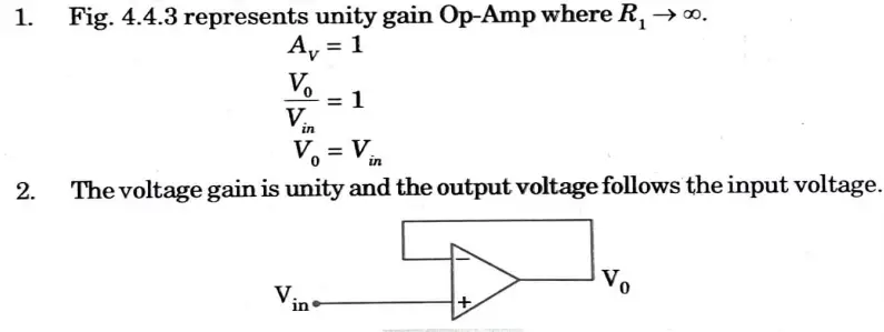
h. What is slew rate explain briefly ?
Ans. Slew rate (SR) : Its greatest rate of output voltage change per unit time, measured in volts per microsecond, is what is meant by the term.
Slew rate describes how quickly an Op-output Amp’s can change in response to an input frequency change.
i. Compare analog and digital instruments.
Ans.
| S. No. | Analog instruments | Digital instruments |
| 1. | Analog instruments are less accurate. | Digital instruments are more accurate. |
| 2. | The sensitivity of analog instruments is more. | Sensitivity of digital instrument is less. |
| 3. | More electricity was required for the analogue instruments. | The power usage was lower for the digital equipment. |
| 4. | The analog instruments are cheap. | The digital instruments are expensive. |
j. Write the applications of CROAns. It is typically employed in laboratories to visualise, quantify, and examine different electrical circuit waveforms.
Section B: Important Questions in Electronic Engineering
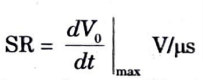
a. Explain Avalanche and Zener Breakdown mechanism.
Ans. Zener breakdown :
- 1. It occurs in a very thin junction (i.e., depletion layer is narrow due to heavily doped junctions on both sides).
- 2. A very strong electric field (about 107 V/m) is created across the thin depletion layer when a tiny reverse bias voltage is applied.
- 3. The covalent bonds can be broken by this field alone. The reverse saturation current is made up of a lot of electrons and holes produced by this breakdown of covalent bonds (i.e., zener current).
- 4. The applied voltage has no effect on the zener current. Only the external resistance influences it.
- 5. As depicted in Fig., this breakdown is known as a zener breakdown. Low voltage causes this failure.
Avalanche breakdown :
- 1. When the connection is somewhat thicker than the case, avalanche breakdown occurs. It indicates that the junction’s two sides are mildly doped.
- 2. For the same applied voltage of the breakdown scenario, the electric field across the depletion zone (layer) in this case is not strong enough to produce zener breakdown zener br.
- 3. Here, the minority carriers accelerated by the field collide with the iconductor atoms in the depletion region.
- 4. The kinetic energy of the electrons involved in a collision is transmitted covalently to other bonds, increasing the pair energy and leading to the covalent bonds being broken and the generation of electron-holes.
- 5. Due to the cumulative process of avalanche multiplication, the newly produced carriers transfer bonds and their energy to other covalent are generated break more bonds, leading to extraordinarily huge numbers of carriers.
- 6. This division At higher voltages, this breakdown, known as avalanche breakdown, as depicted in Fig., takes place.
b. Write a short note on tunnel and varactor diode.
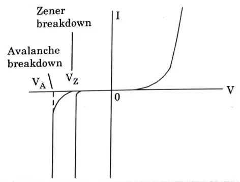
Ans. A. Tunnel diode:
- 1. A small forward bias is applied across the junction.
- 2. Since, the potential of the p-side under this condition is higher than the Potential of n-side EFP will move below EFN as shown in Fig. and the electrons in the conduction band on the n-s1de faces empty states in the valence band on the p-side, at same energy level.
- 3. The thin barrier spanning junction 1 would enable electron tunnelling from the top-side of the n-side, resulting in current flowing from the p-side to the top-side. Therefore, In is true in this instance. More of these filled states would come opposite to the empty states as the forward bias was increased.
- 4. The maximum number of filled states in the conduction band on one side would face the minimum number of empty states in the valence band on the other as the forward bias was increased further. The peak tunnelling current would occur.
- 5. The conduction band of the n-side would migrate away from the valence band of the p-side if the forward bias was increased more, and there would be no vacant states on the p-side that corresponded to the full states on the n-side.
- 6. Due to this, the tunnelling current would eventually reach zero and the normal diffusion component of the current would take over. Normal p-n junction diode properties are the outcome.
B. Varactor diode:
- 1. This is also called as varicap, VVC (voltage variable capacitance), or tuning diode.
- 2. This is made of semiconductor-related components. It is merely a variable capacitor with voltage dependence.
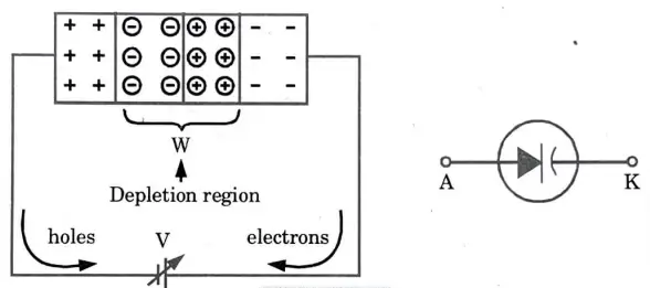
- 3. Fig. shows the varactor diode in reverse-bias condition and symbol of varactor diodes.
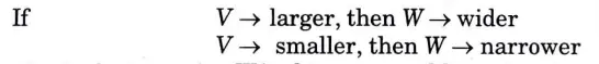
- 4. Similar to the dielectric that separates the two plates of a capacitor, the depletion area W in this case acts as an insulator to impede conduction between the then and p region of the diode.
- 5. Let area of plates = A
If distance between two capacitor plates = W
c. Draw the basic structure of common base BJT and explain its principle of operation with neat diagram with its input and output characteristics.
Ans. Common-base (CB) configuration :
- The input signal is applied between the base and the emitter in this setup. As depicted in Fig., the output is gathered from the collector and base.
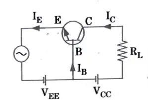
Current amplification factor (α) : 1. It is defined as the ratio of the collect.or current t.o the emitter current of a transistor when no signal is applied and is called DC alpha (αDC).
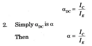
3. In the sense that collector current approaches emitter current, the transistor performs better the higher the value of.
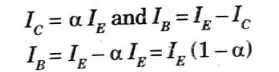
4. The current amplification factor is now defined as the ratio of change in collector to emitter current at constant collector base voltage when a signal is supplied.

6. The collector current can also be expressed as

Input characteristics :
i. There exists a cut in, offset or threshold voltage VBE below which the current is very small.
ii. IE increases rapidly with small increase in VBE i.e., input resistance is very small.
Output characteristics :
i. In active region, the collector current is independent of collector voltage and depends upon emitter current but if VCB increases beyond a certain value, IC increases rapidly due to avalanche breakdown.
In this location, the collector base function is reverse biassed whereas the base emitter function is forward biassed.
ii. In cut off region, a small amount of collector current flows even when IE= 0. i.e., leakage current lCBO.
Here emitter base and collector base junctions both are reversed biased.
iii. In saturation region, current IC flows even if VCB ≅ 0.
Here collector and emitter junctions both are forward biased .
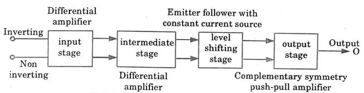
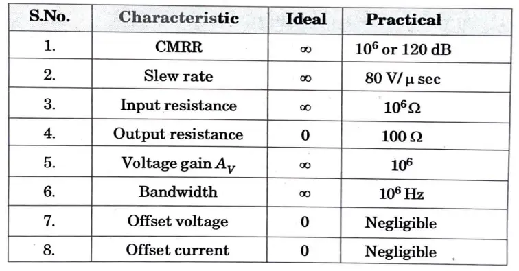
d. Define op-amp with the help of block diagram. List the ideal characteristic of an op-amp. Explain working of op-amp as a Adder.
Ans. A. Block diagram op-amp:
1. Op-amp is designed to perform various mathematical operations.
2. The Fig. represents the block diagram approach of an operational amplifier.
B. Ideal characteristics of op-amp :
C. Op-amp as adder:
1. The three input summer circuit is depicted in Fig. With the help of this circuit, three input voltages that have all been multiplied by a fixed gain factor can be algebraically summed.
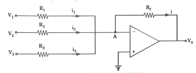
2. At point A (virtual ground), the different currents are given as :
3. Applyin·g KCL at point A, we get,
5. Thus the output voltage is proportional to the algebraic sum of three input voltages.
e. Draw and explain the block diagram of Digital Storage Oscilloscope (DSO) also compare it with analog oscilloscope.
Ans. A. Digital Storage Oscilloscope :
- 1. The input signal is digitalized by a digital oscilloscope, making all subsequent signals also digital.
- 2. Storage takes place in electronic digital memory, which is shown on a traditional CRT.
- 3. Fig. shows a block diagram of a basic digital storage oscilloscope.
- 4. The input signal is converted to digital form and stored in memory. It can be studied in this state to provide a variety of different pieces of information.
- 5. To view the display on the CRT the data from memory is reconstructed in analog form.
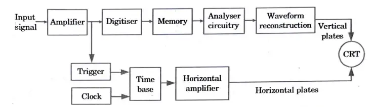
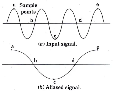
- 6. Digitising occurs by talcing a sample of the input waveform at periodic intervals.
- 7. According to sampling theory, the sampling rate must be at least twice as rapid as the input signal’s maximum frequency in order to prevent information loss. Aliasing will happen as a result if this is not done, as demonstrated in Fig.
- 8. The digitiser, an analogue to digital converter, must have a quick conversion rate in order to meet the demand for a high sampling rate.
- 9. Costly flash analogue to digital converters are typically needed for this, and their resolution degrades as sampling rates rise.
- 10. This is the reason why an analogue to digital converter typically imposes a limit on the bandwidth and resolution of a digital oscilloscope.
B. Comparison:
| S. No. | Analog storage oscilloscope | Digital storage oscilloscope |
| 1. | Its writing speed and bandwidth are higher. | Its writing speed and bandwidth are lower. |
| 2. | CRT used in it, is costlier. | CRT used in it, is cheaper. |
| 3. | Capability of storage time is limited. | Capability of storage time is infinite. |
| 4. | In an analogue oscilloscope, a ramp circuit produces the time base signal. | Crystal clocks produce the time base signal in digital storage oscilloscopes. |
| 5. | It cannot work in look back mode. | It can work in look back mode. |
| 6. | Accuracy is less. | Accuracy is high |
| 7. | Data is collected by analogue oscilloscopes after they have been activated. | Data collection by DSO is constant, and trigger indicates when to stop. |
Section C: Important Long Question in Electronic Engineering Question Paper
a. Draw the V-1 characteristics of an ideal & practical diode and explain. Also write the diode equation in support of your answer
Ans. A. V-1 characteristics of an ideal & practical diode:
- 1. A perfect diode is a conductor when biassed forward and a resistor when biassed backward.
- 2. The current-voltage characteristic of the ideal diode is shown in Fig.
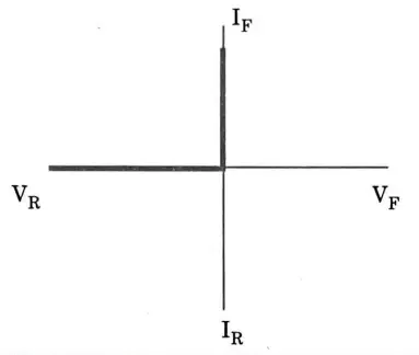
- 3. When a diode is forward biassed, it functions as a short circuit. Reverse bias causes it to function as an open circuit.
- 4. A perfect diode functions as a unilateral switch as a result. In a perfect diode biassed in either direction, no power is lost. As illustrated in Fig., the voltage across the diode is zero in the forward direction, and the current through the diode is zero in the reverse direction.
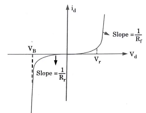
Practical:
- 1. In practical, the battery introduced a small offset voltage (Vr) in forward biased. The value of the offset voltage is determined by the type of semiconductor used in a p-n junction but cannot be measured directly.
- 2. When the diode is ON or OFF, or when the bias is forward or reverse, the resistor comes close to the semiconductor resistance.
- 3. A reverse biased diode conducts a very small amount of current called leakage current.
- 4. Reverse-bias voltage can only be withstood by a diode to a certain extent. The diode will experience significant conduction known as breakdown, which is typically damaging, if the applied reverse-bias voltage grows too big.
- 5. The current versus voltage curve for a real diode looks like as shown in Fig.
B. Diode equation:
1. The V-I characteristic equation, often known as the diode current equation, is a mathematical representation of a diode’s V-I characteristics. It reveals the diode current I and applied voltage V mathematical connection.
2. It is given by,
I = I0[eV/ηVt -1] ………..(1)
where, I0 = Reverse saturation current
V = Applied voltage
η = 1 for Ge diode
= 2 for Si diode
VT = Voltage equivalent of temperature in volts.
3. The element is also known as the ideality or emission coefficient. This element accounts for the recombination effort occurring in the depletion zone.
4. The effect is dominant in silicon diodes and hence for silicon η = 2. The range of factor is from 1 to 2.
5. The voltage equivalent of temperature indicates dependence of diode current on temperature. It is given as,
VT = kT volts …………..(2)
where, k = Boltzmann’s constant = 8.62 x 10⁻⁵ eV/k
T = Temperature in °K
6. The forward biassed and reverse biassed conditions of a diode are both covered by the diode current equation.
i. When unbiased, V = 0 hence we get,
I = I0[e0 -1] = 0 A
Thus, there is no current through diode when unbiased.
ii. For forward biased, V must be taken positive and we get current I positive which is forward current.
iii. For reverse biased, V must be taken negative and we get negative current I which indicates that it is reverse current.
ii. AC or dynamic resistance (rd) :
1. The reciprocal of the slope of a diode’s V-I characteristics is known as AC resistance.
2. It is determined as
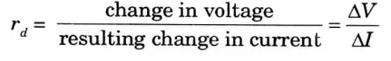
3. A straight line drawn perpendicular to the curve through the Q-point in the diode’s forward characteristics can be used to calculate AC resistance.

4. Lower the Q-point of operation (smaller current or lower voltage), higher is the AC resistance.
5. The Shockley’s equation for the forward and r even:e bias is given by
6. We are aware that the slope of the tangent line drawn at a given location is equal to the derivative of a function at that point.
7. Taking derivative of eq. (1.5.1) with respect to applied voltage V, we get
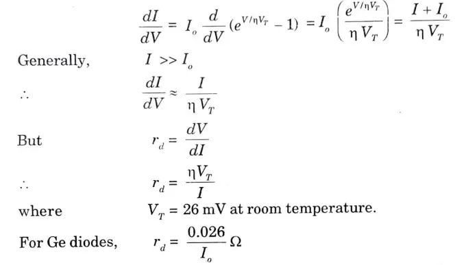
8. AC resistance is the sum of ohmic resistance of the p and n type semiconductor and junction resistance, rj.
iii. Average AC resistance (rav) : If the input signal is significant enough to provide a variety of characteristics, it is the resistance connected to the device for the area.

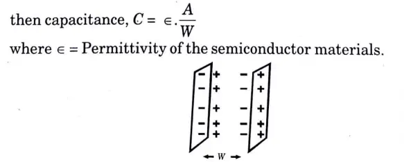
B. Characteristics of transition and diffusion capacitance :
i. Space charge o:t transition capacitance (CT):
- 1. The depletion region functions as an insulator in a reversed biassed p-n junction, while the low resistance p and n-type regions on either side serve as the plate.
- 2. In this way p-n junction may be regarded as parallel plate capacitor.
- 3. The junction capacitance is called space charge capacitance or transition capacitance and is denoted by CT.
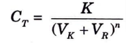
4. Fig. shows the variation of transition capacitance with applied reverse voltage.
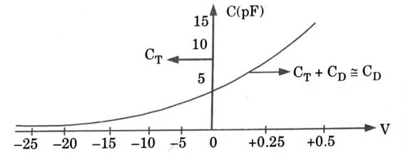

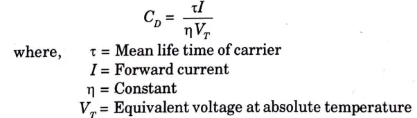
ii. Diffusion or storage capacitance (CD):
- 1. The potential barrier is lowered at p-n junctions that are forward biassed. Now, the electrons from the n-side enter the p-side in a manner identical to how the holes from the p-side enter the n-side.
- 2. These carriers gradually recombine as they disperse away from the junction. When a forward bias voltage is provided, a charge is subsequently stored on both sides of the junction.
- 3. As with a real capacitor, the amount of stored charge fluctuates with the applied potential.
- 4. The diffusion capacitance expressed by the equation CD= dQ/dV, where dQ represents the change in minority carriers stored outside the depletion region when a change in voltage across diode, dV, is applied.
- 5. The diffusion capacitance can be expressed as :
- 6. The value of CD is large for forward current and small for reverse current. Large value of CD delays both the switch-ON and switch-OFF.
Section 4: Important Long Question in Electronic Engineering Question Paper
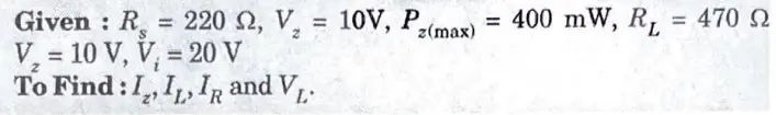
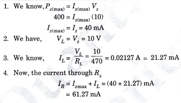
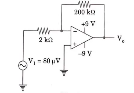
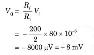
a. Determine Iz, IL, IR, and VL for the network shown in given Fig.1
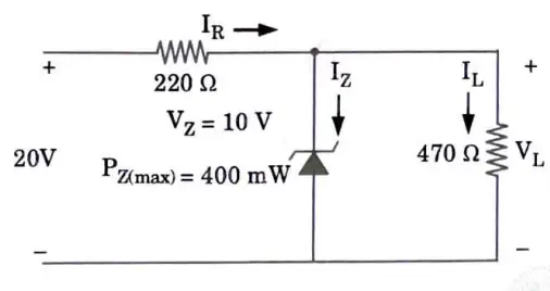
Ans.
b. Determine the output waveform for a given input waveform.
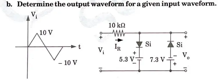
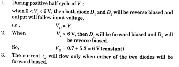
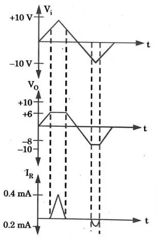
Ans
Section 5 Important Long Question in Electronic Engineering Question Paper
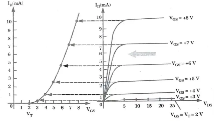
a. Distinguish between enhancement type and depletion type MOSFETs. Draw the cross-section of N-channel enhancement MOSFET. Explain and draw the transfer characteristics.
Ans. A. Difference:

| S. No. | Parameter | Depletion type | Enhancement type |
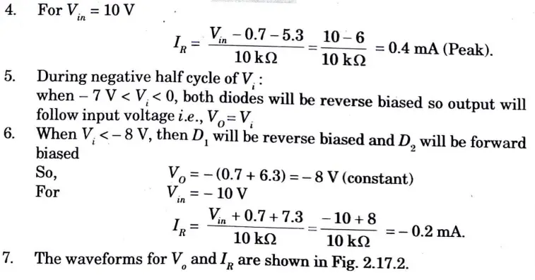
| 1. | Symbols | fig no 1 | fig no 2 |
| 2. | Channel | Exists permanently. | Channel is not present physically. For n-channel enhancement type MOSFETs, it is induced after application of positive gate voltage above the threshold value, while for p-channel enhancement type MOSFETs, it is induced after application of negative gate voltage above the threshold value. |
| 3. | Operation | Can be operated in depletion mode as well as enhance mode. | Can only be operated in enhance mode. |
| 4. | Current flow | Drain current flow on application of drain to source voltage, at VGS = 0. | Practically no current flows on application of drain to Source, at VGS = 0. Current flows only when VGS is above threshold level. |
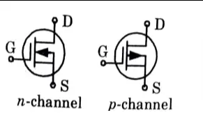
B. N -channel enhancement MOSFET :
Enhancement MOSFET
- 1. Fig. shows the cross-sectional view of n-channel enhancement MOSFET.
- 2. It consists of a lightly doped p -type substrate into which two heavily doped n+-regions are diffused. This n+-regions act as source and drain respectively.
- 3. In order to make metal contacts for the source and drain terminals, holes are bored into the insulating SiO2 layer that has been developed over the whole surface.
- 4. The gate is a conductive layer of aluminium that is layered on the SiO2 layer and spans the entire channel length from source to drain.
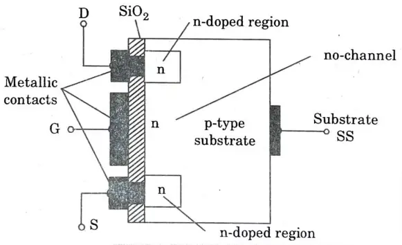
Working of Enhancement MOSFET :
- 1. A parallel plate capacitor is created by the channel, the insulating dielectric SiO2, and the metal layer of the gate.
- 2. Negative charges are induced on the semiconductor side when a positive voltage is applied at the gate with respect to the substrate.
- 3. These unfavourable charges, which are electrons, produce a layer of inversion on a p-type substrate.
- 4. The inversion layer forms an effective n-type channel.
- 5. The size of the induced negative charges in semiconductors grows as the positive voltage at the gate is raised.
- 6. Thus, the conductivity of induced n-channel increases and results in increased drain current.
- 7. For a constant drain voltage, the drain current increases as the positive drain voltage increases i.e., the drain current has been enhanced by the application of positive gate voltage. Such MOSFET is termed as an enhancement MOSFET.
Characteristics curves of enhancement MOSFET :
- 1. Fig. shows the static drain and transfer characteristics of n-channel enhancement MOSFET.
- 2. From Fig. as VGS is made positive, the drain current first increases slowly and then at relatively fast rate with increase of VGS.
- 3. The threshold voltage is defined as the gate voltage at which channel is induced to produce the flow of current ID of prescribed value and is denoted by VT.
- Such type of FET is very useful in switching applications, since no gate voltage is required to hold it off.
Section 6 : Important Long Question in Electronic Engineering Question Paper
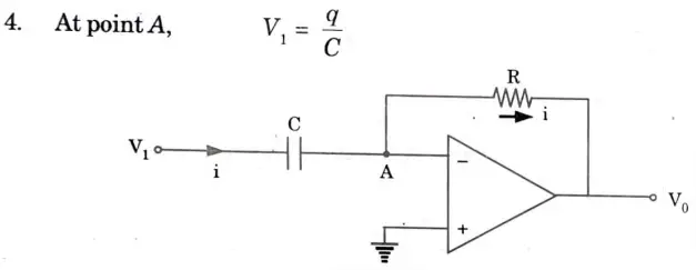
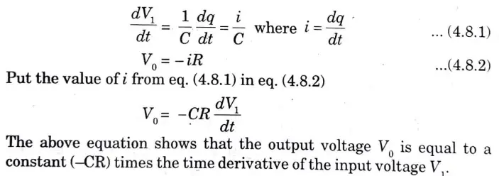
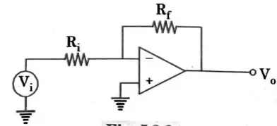
a. Explain the concept of virtual ground. Explain working of Op-Amp as a differentiator.
Ans. A. Virtual ground: A node of a circuit that is at a constant reference potential but is not physically connected to the reference potential is said to have a virtual ground.
B. Op-amp as differentiator:
1. A differentiator’s job is to produce an output voltage that is proportional to the input voltage’s rate of change.
2. The circuit of a differentiator is shown in Fig.
3. We get a constant DC output when we feed the differentiator voltage that is linearly growing. As a result, it is an integrator’s inverse mathematical operation.
b. Determine the output of following Circuits. i.
i.
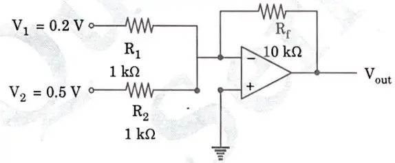
ii.
Ans. i. The given circuit is a summing amplifier, so the output voltage is given by
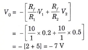
ii. The give circuit is an inverting op-amp, so the output voltage is given by,
Section 7 : Important Long Question in Electronic Engineering Question Paper
a. Describe measurement of voltage, frequency and phase using CRO.
Ans. A. Frequency measurement :
- 1. A Lissajous pattern is produced on the screen when two sinusoidal voltages are supplied to the two sets of deflecting plates.
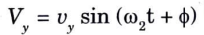
- 2. Let two voltages are Vx and VY at X and Y plates respectively.

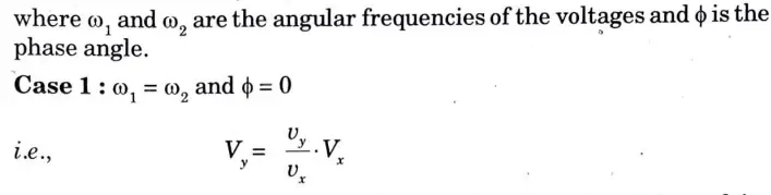
This is an equation of straight line passing through origin and its equivalent is shown in Fig.
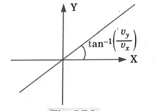

This is an equation of ellipse and its equivalent pattern is shown in Fig.
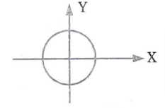
This is the equation of circle and its equivalent pattern is shown in Fig.
- 2. The unknown frequency is applied to Y plates.
- 3. A sinusoidal voltage is applied to X-plates.
- 4. The oscillator’s frequency is adjusted until a single loop stationary pattern appears on the screen.
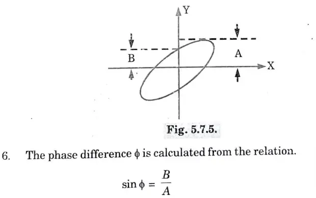
B. Phase measurement :
- 1. Depending on the relative amplitude, frequency, phases, and waveforms of the ac voltages, different patterns can be seen on the CRO screen.
- 2. These patterns are known as Lissajous figures.
- 3. Let consider the case of ellipse.
- 4. The phase difference between two voltages determines how the ellipse will be oriented in relation to the coordinate axes.
- 5. The value of A and Bare noted from the ellipse as shown in Fig.
C. Voltage Measurement (Amplitude Measurement) :
- 1. A calibrated scale for time and amplitude measurements is present on the oscilloscope tube face.
- 2. The boxes are divided into centimetres, with each box further divided into 0.2 cm intervals, 4 cm on either side of the centre.
- 3. The vertical scale is calibrated in either volts per centimeter or millivolts per centimeter.
- 4. We are able to measure peak-to-peak or peak voltage for an AC signal as a result of the scope’s scale setting.
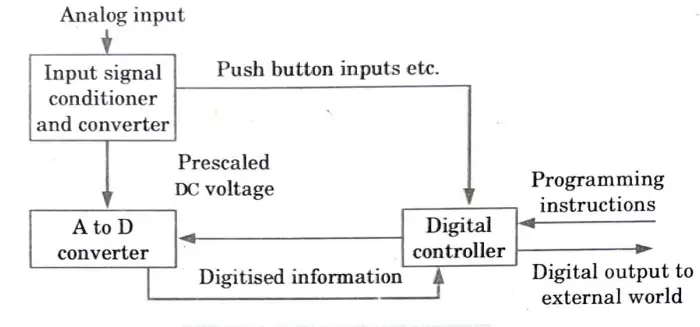
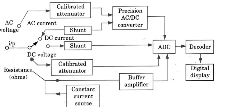
b. Describe the working of Digital Multimeter with their block diagram.
Ans.
- 1. In labs and businesses, the digital multimeter is widely utilised. Fig. depicts the block diagram of a digital multimeter.
- 2. Multimeter is the name of the device used to measure AC/DC voltage, AC/DC current, or resistance values.
- 3. In a typical DMM, the input signal whether an AC or DC voltage, current, resistance, or any other parameter is converted to a DC voltage that falls within the ADC’s dynamic range.
- 4. The pre-scaled DC voltage is next transformed by the ADC into its equivalent digital number, which will be shown on the display device.
- 5. A digital control block, sometimes implemented by a microprocessor or microcontroller, controls the information flow inside the instrument, coordinating all internal operations and sending data via industry-standard interfaces to external devices like printers or personal computers.
Measurement of voltage :In the last question, we talked about the DVM used to monitor voltage.
Measurement of current :
- 1. A number of current sensing resistors are employed for the measurement of current, whether it be AC or DC.
- 2. The current to be measured is passed through one of the sensing resistors as shown in Fig.
3. The output voltage is given by
V0 = -IRf
- 4. The output voltage is proportional to unknown current I.
Here Rf is known resistance.
Measurement of resistance :
1. For the measurement of resistance with DMM, a scale changer is used. A scale changer is shown in Fig.
2. The output voltage of scale changer is given by
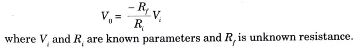
3. When supplied to the digital voltmeter part of the DMM, an unknown resistance, Rf, determines the output voltage. Rf’s value for unknown resistance is shown.
Functions of digital multimeter: Measurement of voltage, current and resistances.
i. Multimeter as voltmeter :
- 1. In the AC voltage mode, the applied AC input voltage is supplied through an attenuator that is compensated, calibrated, and attenuated to a level that is acceptable to subsequent stages.
- 2. A suitable accuracy AC to DC converter converts the attenuated voltage into DC.
- 3. This DC is sent to the ADC, which in turn shows the output in numerical form on the decoder and display system that follows.
ii. Multimeter as ammeter :
- 1. ADC in the DC current mode immediately measures the drop across an internal calibrated shunt after the current is applied to the shunt.
- 2. Accuracy in the AC ranges is often in the range of 0.2 to 0.5% due to the imprecision in the AC/DC conversion.
iii. Multimeter as an ohmmeter :
- 1. When a current is driven through an unknown resistance that is externally connected by a calibrated internal source, a digital multimeter measures the voltage that results.
- 2. Depending on the precision and stability of the internal current source, the accuracy of resistance measurement ranges from 0.1% to 0.5%.
Applications of Digital multimeter:
- a . For checking circuit continuity.
- b. DC voltage across various resistors in an electrical circuit measurement.
- c. AC voltage measurement across the power supply transformer.
- d. to determine whether the circuit under examination has an open or short circuit.

Electronic Engineering Quantum PDF, Syllabus, Important Questions
| Label | Link |
|---|---|
| Subject Syllabus | Syllabus |
| Short Questions | Short-question |
| Important Unit-1 | Unit-1 |
| Important Unit-2 | Unit-2 |
| Important Unit-3 | Unit-3 |
| Important Unit-4 | Unit-4 |
| Important Unit-5 | Unit-5 |
| Question paper – 2021-22 | 2021-22 |
Electronic Engineering Quantum PDF | AKTU Quantum PDF:
| Quantum Series | Links |
| Quantum -2022-23 | 2022-23 |
AKTU Important Links | Btech Syllabus
| Link Name | Links |
|---|---|
| Btech AKTU Circulars | Links |
| Btech AKTU Syllabus | Links |
| Btech AKTU Student Dashboard | Student Dashboard |
| AKTU RESULT (One VIew) | Student Result |
Important Links-Btech (AKTU)
1 thought on “Last Year 2022 Electronic Engineering Question Paper AKTU”