Prepare to ace your AKTU Electronic Engineering exams with our complete set of UNIT-4: OPERATIONAL AMPLIFIERS questions and answers. Improve your chances of success by strengthening your grasp of this critical topic.
Dudes 🤔.. You want more useful details regarding this subject. Please keep in mind this as well.

Important Questions For Electronic Engineering:
*Unit-01     *Unit-02
*Unit-03    *Unit-04
*Unit-05    *Short-Q/Ans
*Question-Paper with solution 21-22
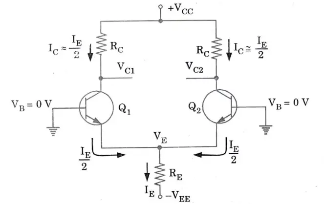
Q1. Draw and explain the differential amplifier circuit.
Ans.
- 1. The emitters are coupled together, and the differential amplifier circuit has two separate inputs and two separate outputs.
- 2. It also consists of two separate voltage supplies.
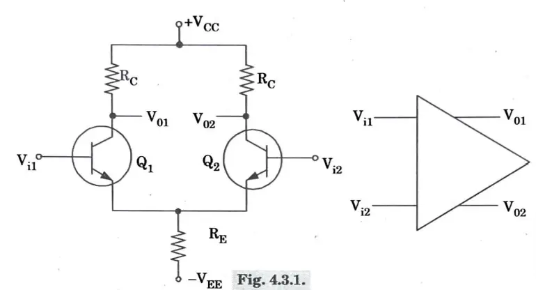
- 3. Due to the common emitter connection in the differential amplifier circuit, the input signal operates both transistors in single-ended mode, producing output from both collectors.
- 4. In a double-ended operation, the difference in the signals applied to the two inputs causes outputs from both collectors when the inputs are different.
- 5. In common-mode operation, a common input signal causes opposite signals to be produced at each collector; these signals cancel one another out and provide a zero as the output signal.
- 6. The primary characteristic of a differential amplifier is its extremely high gain when inputs are provided with opposing signals as opposed to its extremely low gain from common inputs.
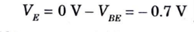
- 7. Let’s consider DC bias operation of the differential amplifier circuit. With each base voltage at 0 V, the common emitter DC bias voltage is
8. The emitter DC bias current is then,
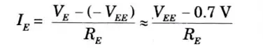
- 9. Assuming the transistors are well matched, we get
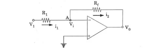
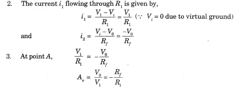
Q2. Draw the circuit of an Op-Amp as voltage follower and find an expression for its voltage gain.
Ans. Inverting Op-Amp :
1. Fig. shows the basic inverting amplifier with input resistance R1 and feedback resistance Rf.
Non-inverting amplifier :
1. The circuit for non-inverting amplifier is shown in Fig.
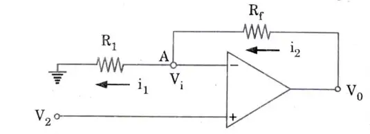
2. The currents i1 and i2 are given as:
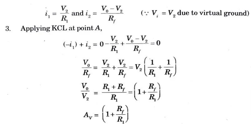
Unity gain Op-Amp (Voltage Follower) :
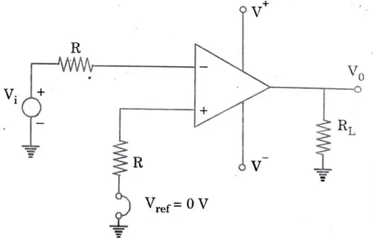
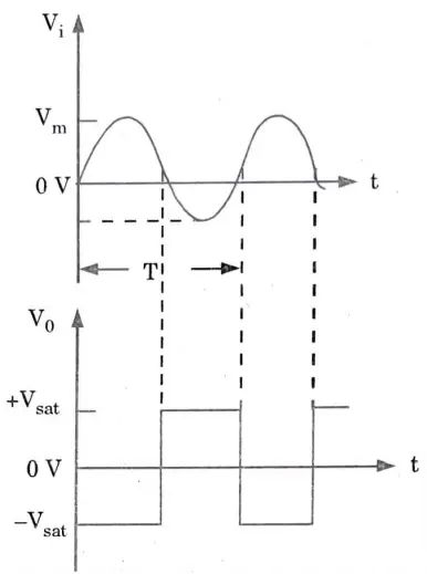
Q3. Explain zero crossing detector using OpAmp.
Ans. When Vref is set to zero, the fundamental comparator can be utilised as a zero crossing detector. A sinusoidal input signal’s output waveform is depicted in Figure together with an inverted zero-crossing detector. The device is additionally known as a sine-to-square wave generator.
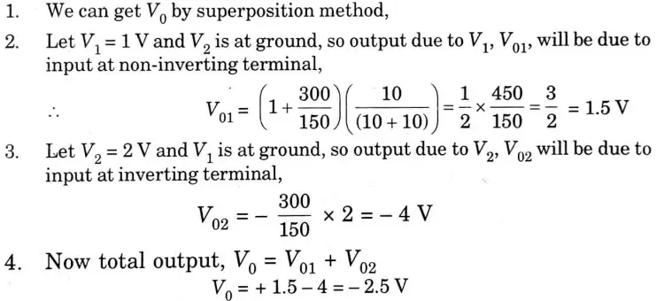
Q4. Determine the output voltage for the given circuit shown in Fig.
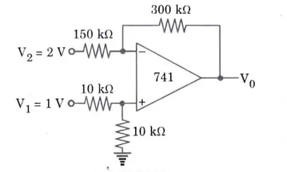
Ans.
Q5. Determine the output voltage for the given Fig.
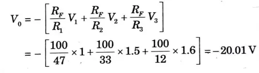
Ans. The output voltage of a summing amplifier is given by
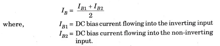
Q6. Explain the basic parameters of Op-amp.
Ans. 1. Input bias current: The input bias currents IB1 and IB2 are the base bias currents of the two transistors in the input differential amplifier stage of the Op-Amp. An input bias current IB is defined as the average of the two input bias currents IB1 and IB2 that is
2. Input offset current and voltage :
i. Input offset current : The input offset current, IiO is defined as the algebraic difference between two input bias currents 1B1 and 1B2

The value of Iw indicates the maximum amount by which the input bias current may differ.
ii. Input offset voltage : The differential input voltage that exists between two input terminals of an Op-Amp when no external inputs are applied is known as input offset voltage, or ViO. In order to force the output voltage to zero, it is the amount of input voltage that needs be applied between two input terminals.
3. Slew rate (SR) : It is defined as the maximum rate of change of output voltage per unit of time and is expressed in volts per micro-second i.e.,
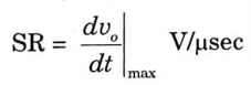
Slew rate describes how quickly an Op-output Amp’s can change in response to an input frequency change.
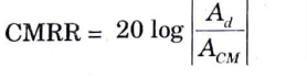
4. CMRR (common-mode rejection ratio) : It is an ability to reject the common mode noise which is present at both the inverting and non-inverting terminal.

Electronic Engineering Quantum PDF, Syllabus, Important Questions
| Label | Link |
|---|---|
| Subject Syllabus | Syllabus |
| Short Questions | Short-question |
| Important Unit-1 | Unit-1 |
| Important Unit-2 | Unit-2 |
| Important Unit-3 | Unit-3 |
| Important Unit-4 | Unit-4 |
| Important Unit-5 | Unit-5 |
| Question paper – 2021-22 | 2021-22 |
Electronic Engineering Quantum PDF | AKTU Quantum PDF:
| Quantum Series | Links |
| Quantum -2022-23 | 2022-23 |
AKTU Important Links | Btech Syllabus
| Link Name | Links |
|---|---|
| Btech AKTU Circulars | Links |
| Btech AKTU Syllabus | Links |
| Btech AKTU Student Dashboard | Student Dashboard |
| AKTU RESULT (One VIew) | Student Result |