Prepare yourself for your Electronic engineering exams with crucial questions and answers from Unit 1: Semiconductor Diodes for AKTU students. For evaluate success, improve your knowledge of diode characteristics, rectifiers, and other topics.
Dudes 🤔.. You want more useful details regarding this subject. Please keep in mind this as well. Important Questions For Electronic Engineering: *Unit-01 *Unit-02 *Unit-03 *Unit-04 *Unit-05 *Short-Q/Ans *Question-Paper with solution 21-22
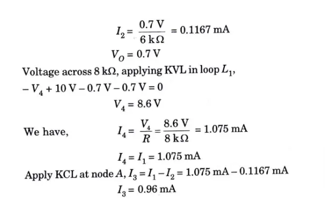
Q1. For the circuit shown in Fig., determine I1 I2, I3, I4, VO.
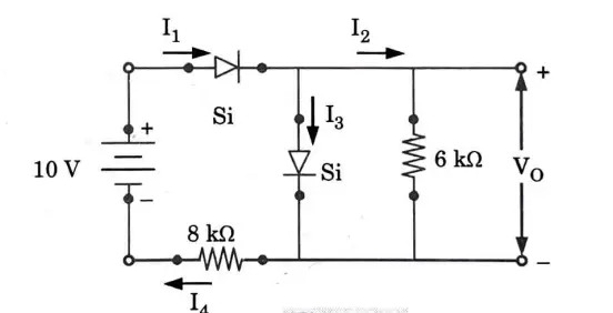
![the circuit shown in Fig., determine I1 I2, I3, I4, VO](https://bachelorexam.com/wp-content/uploads/2023/04/image-565.png)
Ans.
![the circuit shown in Fig., determine I1 I2, I3, I4, VO](https://bachelorexam.com/wp-content/uploads/2023/04/image-565.png)
![the circuit shown in Fig., determine I1 I2, I3, I4, VO](https://bachelorexam.com/wp-content/uploads/2023/04/image-566.png)
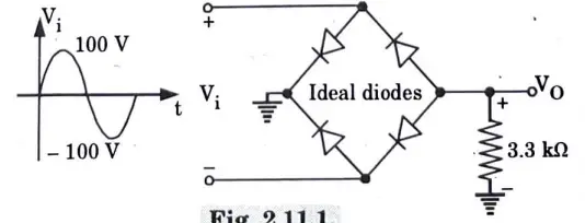
Q2. Sketch VO, VDC for the network of Fig., and determine the peak inverse voltage of each diode.
![Sketch VO, VDC for the network of Fig., and determine the peak inverse voltage of each diode](https://bachelorexam.com/wp-content/uploads/2023/04/image-567.png)
Ans.
![Sketch VO, VDC for the network of Fig., and determine the peak inverse voltage of each diode](https://bachelorexam.com/wp-content/uploads/2023/04/image-569.png)
![Sketch VO, VDC for the network of Fig., and determine the peak inverse voltage of each diode](https://bachelorexam.com/wp-content/uploads/2023/04/image-568.png)
![Sketch VO, VDC for the network of Fig., and determine the peak inverse voltage of each diode](https://bachelorexam.com/wp-content/uploads/2023/04/image-571.png)
![Sketch VO, VDC for the network of Fig., and determine the peak inverse voltage of each diode](https://bachelorexam.com/wp-content/uploads/2023/04/image-570.png)
Peak inverse voltage of each diode = Vm = 100 V
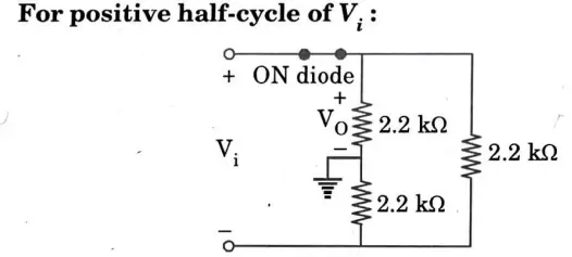
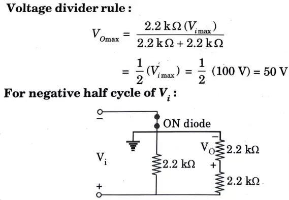
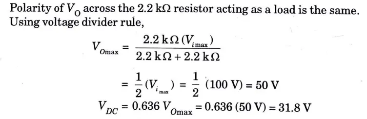
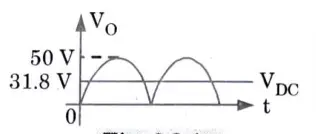
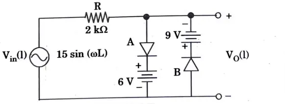
Q3. Determine VO and the required PIV rating of each diode for the configuration of Fig.
![Determine VO and the required PIV rating of each diode for the configuration of Fig](https://bachelorexam.com/wp-content/uploads/2023/04/image-572.png)
Ans.
![Determine VO and the required PIV rating of each diode for the configuration of Fig](https://bachelorexam.com/wp-content/uploads/2023/04/image-573.png)
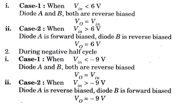
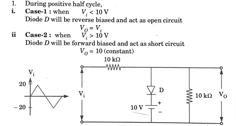
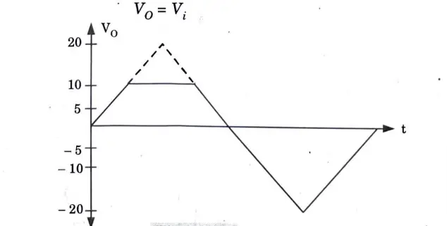
Q4. Explain the function of the circuit of Fig. and draw the output waveform.
![Explain the function of the circuit of Fig. and draw the output waveform](https://bachelorexam.com/wp-content/uploads/2023/04/image-574.png)
Ans. 1. During positive half cycle
![Explain the function of the circuit of Fig. and draw the output waveform](https://bachelorexam.com/wp-content/uploads/2023/04/image-575.png)
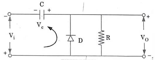
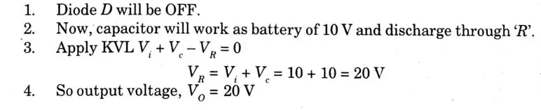
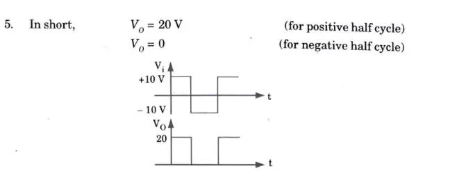
Q5. Draw the output waveform for the following circuits for the input waveforms, given in F. (a) and (b):
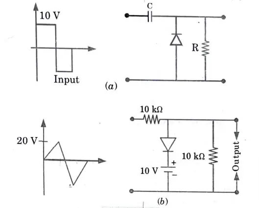
![waveform for the following circuits for the input waveforms](https://bachelorexam.com/wp-content/uploads/2023/04/image-576.png)
Ans. For Fig. (a),
During negative cycle of input :
1. Diode will be ON, capacitor starts charging with polarity as shown in Fig.
![Draw the output waveform for the following circuits for the input waveforms](https://bachelorexam.com/wp-content/uploads/2023/04/image-578.png)
2. The diode will act as short circuit, therefore
VO =0 and VC= +10 V
During positive half cycle :
![Draw the output waveform for the following circuits for the input waveforms](https://bachelorexam.com/wp-content/uploads/2023/04/image-577.png)
![Draw the output waveform for the following circuits for the input waveforms](https://bachelorexam.com/wp-content/uploads/2023/04/image-579.png)
Output waveform of Fig. (b):
![Draw the output waveform for the following circuits for the input waveforms](https://bachelorexam.com/wp-content/uploads/2023/04/image-581.png)
2. During entire negative half cycle, diode will be reverse biased. Therefore
![Draw the output waveform for the following circuits for the input waveforms](https://bachelorexam.com/wp-content/uploads/2023/04/image-580.png)
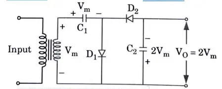
Q6. What is voltage multiplier using p-n junction diode ? Explain the operation of voltage doublers.
Ans.
- 1. The term “voltage multiplier” refers to a circuit that uses a rectifier circuit to produce a higher DC output voltage than AC input voltage.
- 2. The output of voltage doubler is twice the peak input voltage.
- 3. There are two types of voltage doubler circuits:
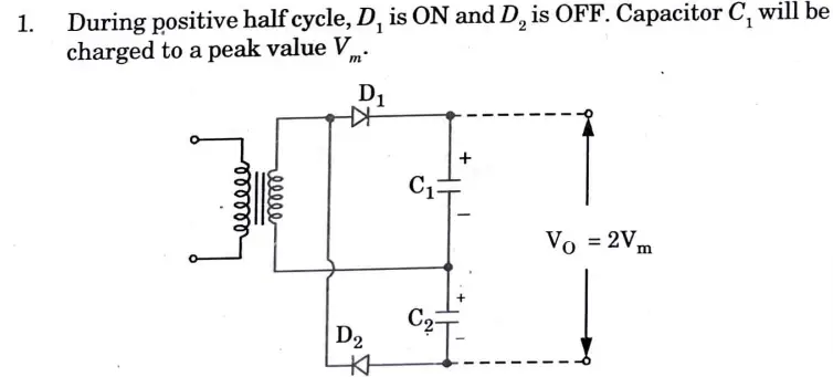
i. Half wave voltage doubler: The circuit diagram is shown in Fig.
![Half wave voltage doubler](https://bachelorexam.com/wp-content/uploads/2023/04/image-582.png)
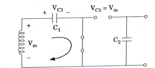
- 1. During positive half-cycle of the input voltage, diode D1 is forward biased (ON) and diode D2 is reverse biased (OFF). Capacitor C1 charges to the peak value of secondary voltage Vm with polarity.
- 2. During negative half-cycle, diode D2 is ON while diode D1 is OFF. Capacitor C2 is charged upto a voltage i.e., the sum of peak-supply voltage and the voltage across C1.
- 3. During positive half-cycle: VC1 = Vm
![What is voltage multiplier using p-n junction diode ? Explain the operation of voltage doublers](https://bachelorexam.com/wp-content/uploads/2023/04/image-583.png)
![What is voltage multiplier using p-n junction diode ? Explain the operation of voltage doublers](https://bachelorexam.com/wp-content/uploads/2023/04/image-584.png)
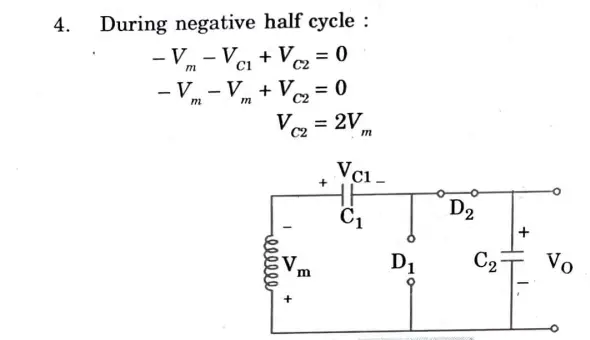
ii. Full wave voltage doubler : The circuit diagram is shown in Fig.
![What is voltage multiplier using p-n junction diode ? Explain the operation of voltage doublers](https://bachelorexam.com/wp-content/uploads/2023/04/image-585.png)
VC1 = Vm
2. During negative half cycle, D1 is OFF and D2 is ON. Capacitor C2 is charged to peak value Vm. Thus output voltage with no load connected :
VO = VC1 + VC2 VO = 2Vm
![AKTU Quantums Pdf Important Notes 2023](http://bachelorexam.com/wp-content/uploads/2023/01/developer-api.jpg)
Important Question with solutions | AKTU Quantums | Syllabus | Short Questions
Electronic Engineering Quantum PDF, Syllabus, Important Questions
Label | Link |
---|---|
Subject Syllabus | Syllabus |
Short Questions | Short-question |
Important Unit-1 | Unit-1 |
Important Unit-2 | Unit-2 |
Important Unit-3 | Unit-3 |
Important Unit-4 | Unit-4 |
Important Unit-5 | Unit-5 |
Question paper – 2021-22 | 2021-22 |
Electronic Engineering Quantum PDF | AKTU Quantum PDF:
Quantum Series | Links |
Quantum -2022-23 | 2022-23 |
AKTU Important Links | Btech Syllabus
Link Name | Links |
---|---|
Btech AKTU Circulars | Links |
Btech AKTU Syllabus | Links |
Btech AKTU Student Dashboard | Student Dashboard |
AKTU RESULT (One VIew) | Student Result |
3 thoughts on “Unit 02 DIODE APPLICATION, Electronic Engineering Qs & Solutions AKTU”