
Are you looking for a comprehensive resource to assist you in preparing for the Computer Organization and Architecture exam? Check out the AKTU B.Tech. Previous Year Computer Organization and Architecture Question Paper. This paper includes a variety of problems covering areas such as input/output, memory, control unit, arithmetic and logic unit, and others. The extensive responses to the questions make it a great resource for test preparation. Whether you want to sharpen your knowledge or need a review on key ideas, this question paper will help you succeed.
Dudes 🤔.. You want more useful details regarding this subject. Please keep in mind this as well.

Important Questions For Computer Organization and Architecture:
*Unit-01     *Unit-02
*Unit-03    *Unit-04
*Unit-05    *Short-Q/Ans
*Question-Paper with solution 21-22
Section A Short Questions with Answer AKTU
a. List and briefly define the main structural components of a computer.
Ans. a. Input unit : The user enters data and programmes into the computer system using this device to process them.
b. Storage unit : Before and after processing, data and instructions are stored in the storage unit.
c. Output unit : The result that the computer produces as output after processing is stored in the output unit.
d. Processing unit : Processing is the process of carrying out operations such as arithmetic and logical processes.
b. Differentiate between horizontal and vertical microprogramming.
Ans.
| S. No. | Horizontal microprogramming | Vertical microprogramming |
| 1. | When using horizontal micro-programming, each bit of the micro-instruction is connected to a particular micro-operation (bit I to represent micro-operation I). | When vertical microprogramming is used, each line of the microprogram represents a micro-instruction that defines one or more microoperations. |
| 2. | Only if the matching bit is set to one does a given micro-operation get carried out during a microinstruction step. | Each stage of the control sequence involves the execution of one micro-instruction. For each micro-operation, a straight binary code can be used to specify it. |
c. Represent the following conditional control statements by two register transfer statements with control functions.

Ans.
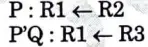
d. Design a 4-bit combinational incremental circuit using four full adder circuits.
Ans.
e. Differentiate between Daisy chaining and centralized parallel arbitration.
Ans.
| S. No. | Daisy Chaining | Centralized Parallel Arbitration |
| 1. | All bus masters use the same line to make bus requests in this straightforward, less expensive approach. | The devices use various request lines to independently request the bus in the centralized, parallel arbitration mechanism. |
| 2. | The daisy chain arbitration that passes through each device in order of decreasing priority. | A centralized arbiter selects one of the devices requesting bus access, notifying the chosen device over one of the grant lines that it is now the bus master. |
f. What is the transfer rate of an eight-track magnetic tape whose speed is 120 inches per second and whose density is 1600 bits per inch?
Ans. The tape moves at a speed s = 120 inches/second
Density of tape= 1600 bits per inch.
Total number of tracks = 8.
Data transfer rate per each track= Tape speed x Density of tape.
= 120 * 1600 = 192000 bits / second.
Hence Data transfer speed per track = 24000 Bytes/ second.
( ∵ 8 bits = 1 byte)
Data transfer speed for 8 tracks = 24000 * 8 bytes / second.
= 192000 bytes I second= 192 KBytes I second.
( ∵ 1000 = 1 Kilo for speed calculation)
g. Register A holds the binary values 10011101. What is the register value after arithmetic shift right ? Starting from the initial number 10011101, determine the register value · after arithmetic shift left, and state whether there is an overflow.
Ans. R = 10011101
Arithmetic shift right: 11001110
Arithmetic shift left : 00111010 overflow because a negative number changed to positive.
h. What is an Associative memory ? What are its advantages and disadvantages ?
Ans. Associative memory :
- 1. When using associative memory, a location is accessible by a field of data words that are stored there rather than by any addresses..
- 2. It can be thought of as a random access memory with built-in bit comparison logic in addition to a physically wired addressing mechanism.
- 3. With the help of a specific input key, this logic circuit permits comparison of the necessary bit positions across all words.
- 4 This comparison is done simultaneously for all the words.
- 5. This is also called Content Addressable Memory (CAM).
Advantages :
- 1. This is suitable for parallel searches.
- 2. It is also used where search time needs to be short.
- 3. It is very high speed searching application.
Disadvantages :
- 1. Associative memory is more expensive than a random access memory.
- 2. Each cell needs to be equipped with additional storage space as well as logic circuitry for comparing its contents to outside arguments.
- 3. Associative memories are typically utilized in situations where the search time is extremely important and needs to be extremely brief.
i. Differentiate between static RAM and Dynamic RAM.
Ans.
| S. No. | Static RAM | Dynamic RAM |
| 1. | Static RAM contains less memory cells per unit area. | In comparison to static RAM, dynamic RAM has more memory cells per unit of space. |
| 2. | It has less access time hence faster memories | Its access time is greater than static RAMs. |
| 3. | Cost is more. | Cost is less. |
j. What are the different types of instruction formats ?
Ans. Four types of instructions are available on the basis of referenced address fields:
- 1. Three address instruction
- 2. Two address instruction
- 3. One address instruction
- 4. Zero address instruction
Section B : AKTU Last Year Question paper With Answer
a. A digital computer has a common bus system for 8 registers of 16 bit each. The bus is constructed using multiplexers.
I. How many select input are there in each multiplexer?
II. What is the size of multiplexers needed?
III. How many multiplexers are there in the bus?
Ans. a. Number of registers = 2n , where n = number of selection input lines
Here, number of registers= 8= 23
Therefore, n = 3
Number of selection inputs in each multiplexer = 3
b. Size of multiplexers= Number of registers x 1
Here, Number of registers = 8
Therefore, Size of multiplexers= 8 x 1
c. Number of multiplexers= Number of bits in each register
Here, Number of bits in each register = 16
Therefore, Number of multiplexers in the bus = 16
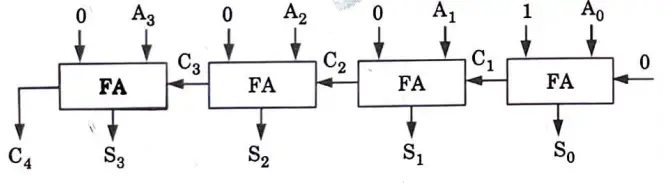
b. Explain destination-initiated transfer using handshaking method.
Ans. 1. In a handshaking process that is begun by the destination, the connection-making process is started by the destination.
2. The handshaking procedure is started by the receiver in this process because the receiver needs to receive the data from the sender.
3. So, in this process, the receiver has to first send the request signal to the source channel.
4. Then, before transferring the data, the source transmits the signal “DATA VALID,” and the receiver follows up by sending the signal “DATA ACCEPTED” after it has received the data.
5. When destination initiates the process of data transfer :
a. REQUEST FOR DATA: If ON requests for putting data on the data bus.
b. DATA VALID: If ON tells data is valid on the data bus otherwise invalid data
Now there is assurance that the data was successfully transferred from the source to the data bus.
Signals can be seen as :
- 1. It demonstrates how the data bus is loaded first, followed by the request for data, and finally the data valid signal.
- 2. First the Request for Data signal goes off after reading the data, then the Data Valid signal.
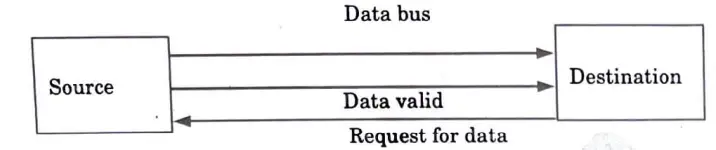
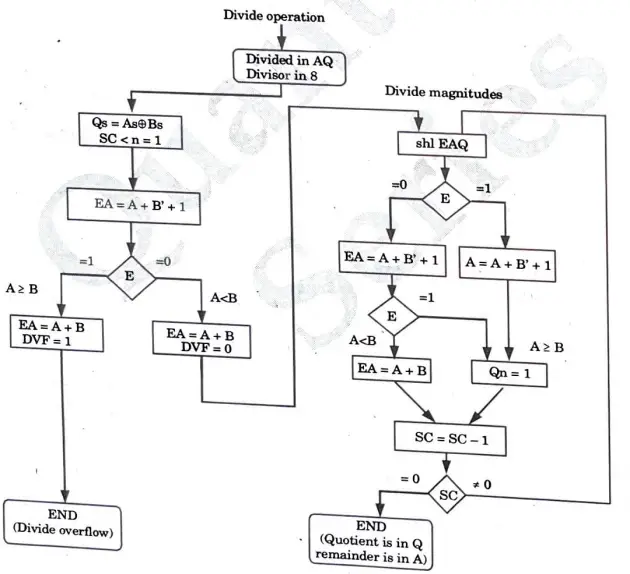
c. Explain 2-bit by 2-bit Array multiplier. Draw the flowchart for divide operation of two numbers in signed magnitude form.
Ans.
- 1. A digital combinational circuit known as an array multiplier is used to multiply two binary values by using an array of full adders and half adders.
- 2. The numerous product keywords involved are added simultaneously using this array.
- 3. Before the Adder array, an array of AND gates is utilized to create the various product terms.
- 4. A series of add and shift micro-operations are needed to perform a sequential operation that involves checking the multiplier’s bits one at a time and creating partial products.
- 5. Consider multiplying two 2-bit values as shown in figure for array multiplier implementation with a combinational circuit.
- 6. The multiplicand bits are b1 and b0 the multiplier bits are a1 and a0 and the product is
Flowchart :
d. A digital computer has a memory unit of 64K X 16 and a cache memory of IK words. The cache uses direct mapping with a block size of four words.
I. How many bits are there in the tag, index, block, and word fields of the address format?
II. How many bits are there in each word of cache, and how they are divided into functions? Include a valid bit.
III. How many blocks can the cache accommodate?
Ans. I. Main memory has 64K = 64 x 1024 = 2 ^ 6 x 2 ^ 10 = 2 ^ 16 words
Cache memory has 1K = 1024 = 2^10 words
In this case to address main memory we need 16 bits (2 ^ 16) and to address cache memory we need 10 bits (2 ^ 10).
So Index is 10 bits wide and Tag is 6 bits wide (16 – 10 = 6).
In this case the block is 4 words long for what we need 2 bits (2 ^ 2) and that leaves 8 bits (10 – 2 = 8) for addressing blocks.
Tag = 6bits
Index = 10 bits
Block = 8 bits
Word = 2 bits
Il. Valid bit = 1 bit
Tag = 6 bits
Data = 16 bits
Total bits = 1 + 6 + 16 = 23 bits
Ill. If cache has 1K words and block size is 4 words then number of blocks is 1K / 4 = 1024 / 4 = 256 blocks.
e. Explain with neat diagram, the address selection for control memory.
Ans.
- 1. The control memory required the capabilities of address sequencing, which is described as follows :
- a. The address sequencing chooses the conditional branch or unconditional branch based on the status bit circumstances.
- b. Addressing sequence is able to increment the CAR (Control address register).
- c. It offers the ability to call and return from subroutines.
- d. The addressing sequence from the instructions’ bits to a control memory address offers a mapping method.
- 2. The block diagram of a control memory and associative hardware, which are needed to choose the address of the subsequent microinstruction, is shown above.
- 3. A group of bits are stored in the control memory using the micro-instruction. We can initiate the microoperations in a computer register with the aid of a few bits.
- 4. The remaining micro-instruction bits are utilised to define the process by which we can find the next address.
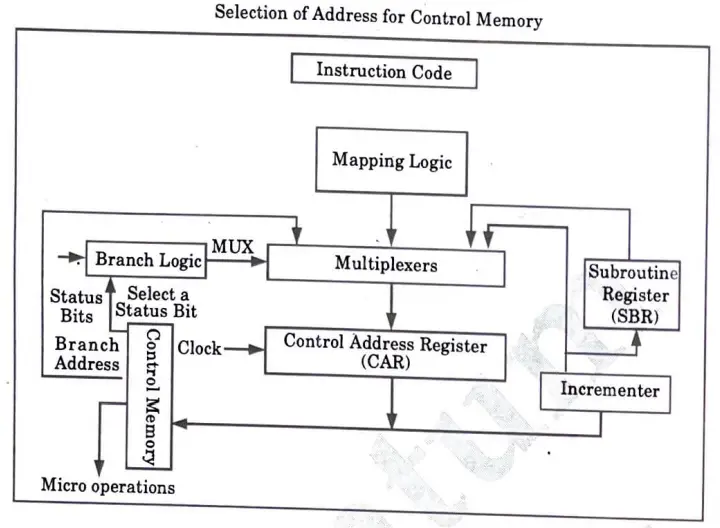
- 5. We can also see in this diagram that the control address register can find its address using four distinct approaches.
- 6. The CAR is incremented with the help of incrementer and then chooses the next instruction.
- 7. In order for the branching results to be provided, the branching address will be decided in the various fields of microinstruction.
- 8. In this situation, conditional branching can be used if there are status bits in the micro-instructions and we wish to apply conditions to them.
- 9. A mapping logic circuit can be used to share an external address. A unique register will save the return address.
- 10. When the microprogram needs to exit the subroutine, his saved address will be useful. The value from the unique register is then needed.
Section C | Q3 to Q7 Important Question With Answer
a. A binary floating-point number has seven bits for a biased exponent. The constant used for the bias is 64.
I. List the biased representation of all exponents from – 64 to +63.
II. Show that after addition of two biased exponents, it is necessary to subtract 64 in order to have a biased exponent’s sum.
III. Show that after subtraction of two biased exponents, it is necessary to add 64 in order to have a biased exponent’s difference.
Ans. a. e = exponent e + 64 = biased exponent
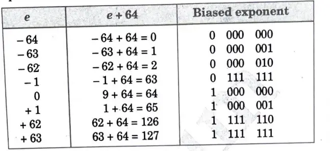
b. The biased exponent follows the same algorithm as a magnitude comparator.
c. (e1 + 64) + (e2 + 64) = (e1 + e2 + 64) + 64
subtract 64 to obtain biased exponent sum
d. (e1 +64)-(e2 -64)=e1 +e2
add 64 to obtain biased exponent difference
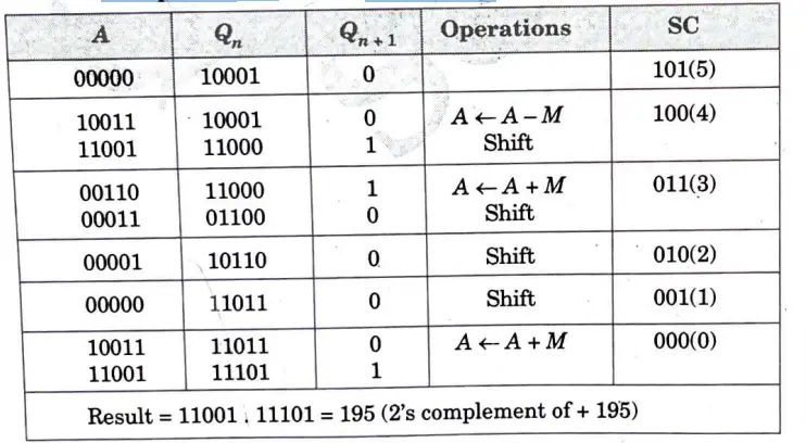
b. Show the multiplication process using Booth algorithm, when the following binary numbers, (+13) x (- 16) are multiplied.
Ans. 13 = 01101
– 15 = 2’s complement of 15 = 10001
Multipiicard (M) = 01101, Multiplier= 10001
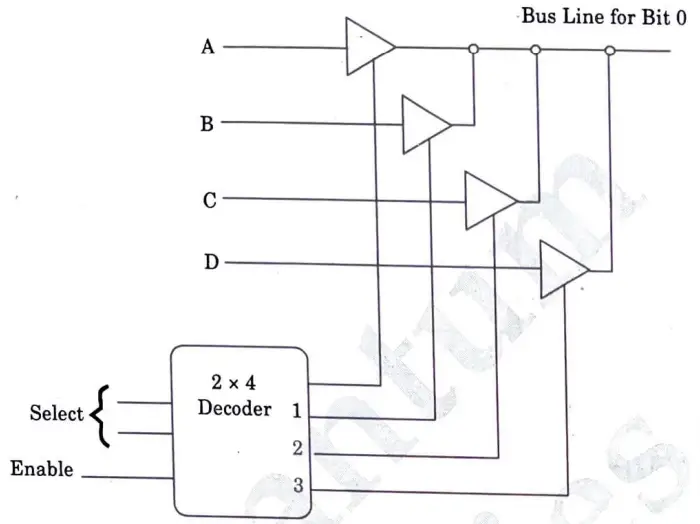
4a. Draw a diagram of a Bus system in which it uses 3 state buffers and a decoder instead of the multiplexers.
Ans.
4b. Explain in detail multiple bus organization with the help of a diagram.
Ans. Multiple-Bus Organization : .
- 1. Two buses are utilized in organizations that operate multiple buses as independent communication channels.
- 2. Both data and instruction transfer take place in many buses in organizations with multiple buses.
- 3. Multiple bus organization has more number of associated registers.
- 4. Two operands can be read from the bus using multiple bus organizations.
- 5. This system operates more quickly because numerous devices cooperate to deliver superior performance.
- 6. A multi-core processor is used in multiple bus organisations to transfer more data and information while reducing wait times.
Diagram:
- 1. Fig. 5 shows a three bus structure used to connect the register and the ALU of the processor.
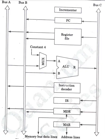
- 2. The register file is a single block that contains all general purpose registers.
- 3. There are three ports on it. There are two outputs, allowing simultaneous access to the contents of two distinct registers and placement of those values on buses A and B. The third port enables the same clock cycle to be used to load data from bus C into a third register.
- 4. The source operands are transferred through Bus A and B to the A and B inputs of the ALU, where arithmetic or logical operations may be carried out.
- 5. The result is transferred to the destination over bus C.
- 6. Incrementer unit, which is used to increment the PC by 4.
5a. The logical address space in a computer system consists of 128 segments. Each segment can have up to 32 pages of 4K words each. Physical memory consists of 4K blocks of 4K words each. Formulate the logical and physical address formats.
Ans. Logical address space has 128 segments x 32 pages x 4 K words
i.e., 128 X 32 X 4 X 210
= 27 x 25 x 22 x 210 = 224 = 24 bit
Physical memory has address space of 4 K blocks x 4 K words
= 4 X 210 X 4 X 210
= 224 = 24 bits
∴ Address format for logical address :
Segment addressing: 7 bits
Page addressing= 5 bits
Word addressing= 12 bits
∴ Address format for physical address :
Block addressing = 12 bit
Word addressing= 12 bit
5b. How is the Virtual address mapped into physical address ? What are the different methods of writing into cache ?
Ans. Mapping Virtual Addresses to Physical Addresses :
1. A hardware component known as MMU performs the mapping between virtual address and physical address at runtime.
2. The Operating System will take care of memory management and transport processes between disc and memory for execution.
3. It keeps track of available and used memory
MMU scheme:
CPU——- MMU——Memory
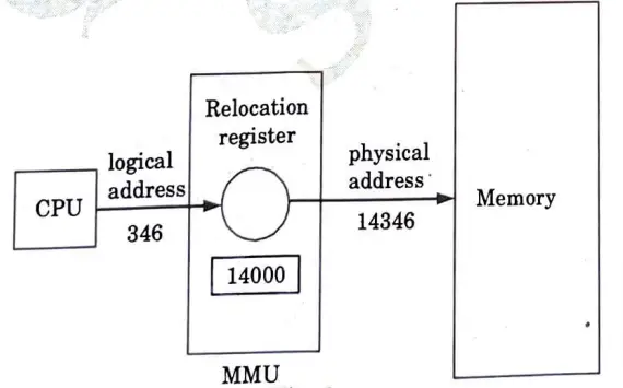
- 1. CPU will generate logical address for example : 346
- 2. MMU will generate a relocation register (base register) for example: 14000.
- 3. In memory, the physical address is located example : (346+ 14000 = 14346)
- 4. Every address generated by a user process has the value from the relocation register appended to it at the moment the address is transferred to memory.
- 5. The actual physical addresses are never visible to the user software.
- 6. In the same way that the number 346 can be created, stored in memory, modified, and compared to other addresses, the programme can also generate a pointer to position 346.
- 7. Only logical addresses are generated by the user programme. Before being used, these logical addresses must to be mapped to physical addresses.
Different methods of writing into cache :
i. Write through:
- a. This is simplest technique
- b. This method ensures that main memory is always valid by performing all write operations both to main memory and the cache.
- c. This method’s primary drawback is the amount of memory traffic it produces, which could lead to a bottleneck.
ii. Write back:
- a. It is another technique which minimizes memory writes.
- b. With write back, updates are made only in the cache.
- c.A slot’s UPDATE bit is set whenever an update takes place. If and only if the UPDATE bit is set, a block is then written back to main memory after being replaced.
- d. The issue with write back is that certain areas of main memory are incorrect, making the only way for I/O modules to access them the cache.
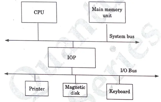
6a. Explain how the computer buses can be used to communicate with memory and 1/0. Also draw the block diagram for CPU-IOP communication.
Ans. There are three ways that computer buses can be used to communicate with memory and I/O :
1. Use two separate buses, one for memory and the other for I/O:
- a. A separate set of data, address, and control buses, one for accessing memory and the other for I/O, are present in this instance.
- b. Computers that offer an additional I/O processor (IOP), also known as an I/O channel, in addition to the CPU, employ this approach.
- c. Through a memory bus, the memory communicates with both the CPU and the 10P.
- d. The IOP’s goal is to offer a distinct conduit for data transfer between external I/O devices and internal memory.
2. Use one common bus for both memory and I/O but have separate control lines for each :
- a. Computers in this scenario send data between memory or I/O and the CPU using a single, shared bus.
- b. Separate read and write lines are used to differentiate between memory transfers and I/O transfers.
- c. By turning on one of two possible read or write lines, the CPU indicates whether the address on the address Imes is for a memory word or for an interface register. During an I/O transfer, the I/O-read and I/O-write control lines are activated.
- d During a memory transfer, the memory read and memory write control lines are turned on. It is known as the isolated I/O or I/O mapped I/O method for allocating addresses in a common bus because it separates all I/O interface addresses from the addresses assigned to memory.
3. Use one common bus for memory and I/O with common control lines :
- a. Computers in this scenario do not differentiate between memory and I/O addresses and use a single set of read and write signals.
- b. This configuration is referred to as memory mapped I/O.
- c. An I/O interface register is regarded by the processor as a component of the memory system.
- d. In other words, the CPU represents the I/O interface using a subset of the memory addresses.
The block diagram foe CPU-IOP communication:
6b. What are the different methods of asynchronous data transfer ? Explain in detail.
Ans. Different methods of asynchronous data transfer :
1. Strobe control method :
- a. A single control line is used to time each transfer in the strobe control method of asynchronous data transfer.
- b. Depending on who initiates the transfer, either the source or the destination may obtain this control line, often known as a strobe.
a. Source initiated Strobe : when the source starts the data transfer process. Simply a signal, a strobe is.
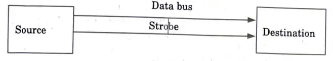
- i. The source turns on the strobe signal and then transfers data to the data bus.
- ii. Read data from the data bus when you detect the strobe’s ON signal at the destination.
- iii Strobe turns off after reading data from the data bus according to destination.
Signals can be seen as : Fig. shows that first data is put on the data bus and then strobe signal gets active.
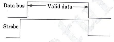
b. Destination initiated signal : When destination initiates the process of data transfer.

- i. To confirm that the source is putting new data on the data bus, the destination must first turn on the strobe signal.
- ii. When the source detects the ON signal, it updates the data on the data bus.
- iii. Destination receives an OFF signal and reads the data from the data bus.
Signals can be seen as : Fig. shows that first strobe signal gets active then data is put on the data bus.
2. Handshaking method :
- a. A second control signal line that replays the unit that started the transfer is added via the handshaking technique.
- b. One control line in this method runs from the source to the destination in the same direction as the data flow in the bus. It is used by the source unit to let the destination unit know whether the bus contains any valid data.
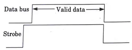
a. Source initiated Handshaking: When source initiates the data transfer process. It consists of signals :
1. DATA VALID : if ON tells data on the data bus is valid otherwise invalid.
2. DATA ACCEPTED : if ON tells data is accepted otherwise not accepted.

- i. Source enables the Data Valid signal and loads data onto the data bus.
- ii. Destination enables the Data Accepted signal and accepts data from the data bus.
- iii. Following that, disable Data bus invalidation is indicated by a data valid signal.
- iv. Disable Data accepted signal and the process ends.
Signals can be seen as : It demonstrates that data is loaded onto the data bus first, followed by the activation of the data valid and data accepted signals. After accepting the data, the data accepted signal disappears first, followed by the data valid signal.
2. Destination initiated handshaking :
- 1. In a handshaking process that is begun by the destination, the connection-making process is started by the destination.
- 2. The handshaking procedure is started by the receiver in this process because the receiver needs to receive the data from the sender.
- 3. Therefore, the receiver must first transmit the request signal to the source channel in this operation.
- 4. Then, before transferring the data, the source transmits the signal “DATA VALID,” and the receiver follows up by sending the signal “DATA ACCEPTED” after it has received the data.
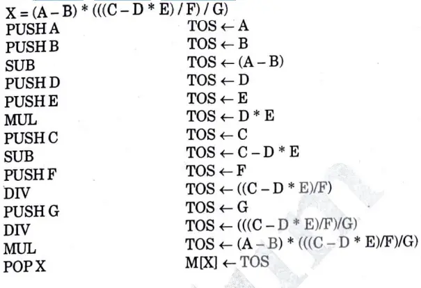
7a. Write a program to evaluate arithmetic expression using stack organized computer with 0-address instructions.
X= (A-B) * (((C-D * E) /F) /G)
Ans. X= (A-B) * (((C-D * E) /F) /G)
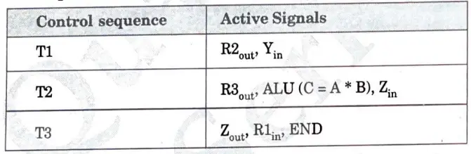
7b. List the differences between hardwired and micro programmed control in tabular format. Write the sequence of control steps for the following instruction for single bus architecture.
R1 ← R2* (R3)
Ans. Difference:
| S. No. | Characteristics | Hardwired control | Micro-programmed control |
| 1. | Speed | Fast | Slow |
| 2. | Implementation | Hardware | Software |
| 3. | Flexibility | Not flexible | Flexible |
| 4. | Ability to handle large/ complex instruction set | Somewhat difficult | Easier |
| 5. | Ability to support operating system and diagnostic features | Very difficult | Easy |
| 6. | Design process | Difficult for more operation | Easy |
| 7. | Memory | Not used | Control memory used (RAM or ROM) |
| 8. | Chip area efficiency | Uses less area | Uses more area |
| 9. | Used in | RISC processor | CISC processor |
| 10. | Output generation | On the basis of input signal | On the basis of control line. |
Sequence:

Computer Organization and Architecture Quantum PDF, Syllabus, Important Questions
| Label | Link |
|---|---|
| Subject Syllabus | Syllabus |
| Short Questions | Short-question |
| Important Unit-1 | Unit-1 |
| Important Unit-2 | Unit-2 |
| Important Unit-3 | Unit-3 |
| Important Unit-4 | Unit-4 |
| Important Unit-5 | Unit-5 |
| Question paper – 2021-22 | 2021-22 |
Computer Organization and Architecture Quantum PDF | AKTU Quantum PDF:
| Quantum Series | Links |
| Quantum -2022-23 | 2022-23 |
AKTU Important Links | Btech Syllabus
| Link Name | Links |
|---|---|
| Btech AKTU Circulars | Links |
| Btech AKTU Syllabus | Links |
| Btech AKTU Student Dashboard | Student Dashboard |
| AKTU RESULT (One VIew) | Student Result |
1 thought on “Last Year Computer Organization and Architecture Question Paper AKTU 2023”