
Explore the VLSI Technology Short Question Notes from the B.Tech. AKTU Quantum Book. Discover the fundamentals of IC design, very large scale integration, and cutting-edge fabrication methods for cutting-edge semiconductor technology.
Dudes 🤔.. You want more useful details regarding this subject. Please keep in mind this as well.

Important Questions For VLSI Technology:
*Quantum             *B.tech-Syllabus
*Circulars              *B.tech AKTU RESULT
* Btech 3rd Year   * Aktu Solved Question Paper
Unit-I: Introduction to ICT Technology (Short Question)
Q1. Define small scale integration.
Ans. Small scale integration occurs when there are less than 100 active devices per chip (SSD). Integral resistors, diodes, and bipolar transistors are used in the majority of SSI devices.
Q2. What do you mean by LSI ?
Ans. The range of active devices per chip in large scale integration (LSD) is between 1000 and 10,000. MOS transistors are typically used in LSl chips because they require fewer steps for integration.
Q3. Mention the advantages of integrated circuits.
Ans. 1. Less power consumption.
2. Higher reliability, mainly due to improved on chip interconnection.
3. Significant cost savings.
Q4. What is electronic-grade silicon ? Give its chemical reaction also.
Ans. The starting material for creating single crystal silicon is a polycrystalline substance with a high degree of purity called electronic-grade silicon (EGS).
Chemical equation for overall reaction that place in furnace is:

Q5. Why the Czochralski technique is used ?
Ans. Controlled freezing of a melt in a boat or ampoule can generate single crystals. The potential for the freezing melt to adhere to the walls is a drawback of this method. Special precautions must be taken to reduce the effect of this type of contact, which can lead to the creation of dislocations. Consequently, we employ the Czochralski method.
Q6. Write the points of considerations for proper crystal growth.
Ans. Points of considerations for proper crystal growth are:
- i. Role of point defects.
- ii. Thermal gradient in the crystal.
- iii. Turbulences in the melt.
- iv. Pull and spin rate.
- v. Crystal orientation.
- vi. Crystal hardening techniques.
Q7. Name all the subsystems of puller.
Ans. The Czochralski crystal growth apparatus, also called a “puller” has tour subsystems and they are:
- i. Furnace
- ii. Crystal-pulling mechanism
- iii. Ambient control
- iv. Control system
Q8. List the steps used in the preparation of Si-wafers.
Ans. Steps used in the preparation of Si-wafers:
- 1. Poly-Crystalline Silicon (Nuggets)
- 2. Pulling Single Crystal Silicon Ingots (CZ Method)
- 3. Single Crystal Silicon Ingots
- 4. Slicing
- 5. Beveling (Peripheral Rounding)
- 6. Lapping (Double Side Lapping)
- 7. Etching (Chemical Polishing)
- 8. Heat Treatment to Remove Unstable Donors
- 9. Polishing (Single Side Mirror Polishing)
- 10. Cleaning
Q9. Name the defect in the crystal structure.
Ans. Defects that are present in the crystal structure are :
- i. Point defect,
- ii. location,
- iii. Area (Planar) defect, and
- iv. Volume defect.
Q10. What are the point and dislocation defects in the crystal structure ?
OR
What are point defects ?
Ans. i. Point defects: Any non-silicon atom included in the lattice at a substitutional or interstitial location is regarded as a point defect in this defect.
ii. Dislocation defects: These flaws serve as the nuclei for the precipitation of pollutants like oxygen and cause the swirl pattern in the water.
Q11. What are the area and volume defects in the crystal structure ?
Ans. i. Area (Planar) defects: Area defects, like twins and grain borders, are large-area lattice discontinuities.
ii. Volume defect: When several point defects combine to create a three-dimensional pore or void, they are referred to as volume or three-dimensional flaws. On the other hand, a group of impurity atoms may combine to form a precipitate that is three dimensional.
Q12. Differentiate among point, Frenkel and Schottky defects.
Ans.
| S. No. | Frenkel defects | Schottky defect |
| 1. | It results from ions absent from the lattice sites, which occupy interstitial sites. | It is caused by lattice sites missing an equal number of cations and anions. |
| 2. | It has no defect on the density of crystal. | It results in decrease in density of crystal. |
| 3. | This is found in crystal with low coordination no. For examples: ZnS | This is found in the highly ionic compounds with having cations and anions of same sizes. For examples: NaCl, CaCl |
Q13. Define polishing.
Ans. The final stage of silicon shaping is polishing. Its goal is to offer a slick, shiny surface for photoengraving device features.
Q14. What is the objective of wafer cleaning?
Ans. The goal of wafer cleaning is to eliminate chemical and particle contaminants from the semiconductor surface without harming or negatively affecting the substrate surface.
Q15. Why is cleaning of silicon wafer necessary before any processing steps ?
Ans. Reason :
- 1. It is important to protect the silicon surface from impurities during diffusion, which could adversely affect the profile’s uniformity.
- 2. Localized impurity concentration may be caused by crystal flaws. The junction properties deteriorate as a result of this.
- 3. Hence, it is necessary to make the silicon crystals extremely flawless.
Unit-II: Epitaxy and Oxidation (Short Question)
Q1. What is epitaxy ?
Ans. A thin crystalline layer is grown on a crystalline substrate using a method known as epitaxy. The substrate wafer performs the role of a seed crystal in the epitaxial process.
Q2. What is the difference between pseudo homoepitaxy and heteroepitaxy ?
Ans.
| S. No. | Homoepitaxy | Heteroepitaxy |
| 1. | Homoepitaxy is the epitaxial growth of a material on a substrate made of the same material. | Heteroepitaxy is the term for the procedure where the layer and substrate are made of different materials. |
Q3. List the various aspects of vapor phase epitaxy?
Ans. Various aspects of vapor phase epitaxy are :
- i. Process chemistry.
- ii. Aspects of process hardware.
- iii. Current capabilities.
Q4. What is auto doping in growth process ?
Ans. An improved transition region between the layer and substrate is how it shows up. The solid-state diffusion from the substrate, which is a complementary error function, dominates the shape of the doping profile close to the substrate.
Q5. What are susceptors ?
Ans. Epitaxial reactors’ susceptors are comparable to crucibles in the crystal-growing process. In induction heated reactors, they serve as the source of thermal energy for the reaction as well as mechanical support for the wafers.
Q6. What do you mean by SoI ?
Ans. A modern non-epitaxial method of producing single-crystal silicon is silicon on Insulator. Amorphous or polycrystalline silicon is recrystallized using this process on an amorphous substrate.
Q7. Define misfit dislocations.
Ans. Another kind of defects is misfit dislocations, which result from lattice mismatch when the substrate is heavily doped. The production of dislocations reduces the strain that results between the layer and substrate.
Q8. Write all the three methods for modifying the CVD process.
Ans. Three methods for modifying the CVD process are:
- i. Selective epitaxy
- ii. Gas flows can be started and stopped to manage a traditional epitaxial growth process.
- iii. Plasma excitation is used to achieve growth at temperatures lower than those at which the reaction may be powered using traditional techniques.
Q9. Define the process of oxidation.
Ans. A layer of silicon dioxide is generated on the surface of a silicon wafer by the process of oxidation. Heating silicon wafers in an oxidizing environment, such as oxygen or water vapour, causes silicon to oxidize.
Q10. Explain the purpose of oxidation.
Ans. 1. To act as a shield against the diffusion or implant of dopants into silicon.
2. To give passivation of the surface.
3. The capacity to produce high-quality oxide in a controlled and ideal manner.
Q11. What is preoxidation cleaning ?
Ans. Wafers must be cleaned to remove both organic and inorganic impurities before being put in a high temperature furnace. Preoxidation cleaning is the term for this.
Q12. What is plasma oxidation ?
Ans. Low-temperature vacuum processes like plasma oxidation are typically conducted in pure oxygen discharges.
Q13. How the plasma is produced in the plasma oxidation ?
Ans. The plasma is produced either by high-frequency discharge or a DC electron source.
Q14. How can we increase the growth rate of oxide in the plasma oxidation ?
Ans. In general, as the substrate temperature, plasma density, and substrate dopant concentration rise, so does the oxide’s development rate.
Unit-III: Lithography and Polysilicon Film Deposition (Short Question)
Q1. What is lithograph ?
Ans. A lithograph is a less expensive type of picture created by successively pressing numerous flat, embossed slabs, each covered with a distinct colour of grease ink, onto a sheet of sturdy paper.
Q2. What does optical lithography comprise ?
Ans. Optical lithography is the process of creating images using visible or ultraviolet light in a photoresist through proximity, contact, or projection printing.
Q3. Write the advantages of electron lithography over optical lithography.
Ans. Advantages of electron lithography over optical lithography:
1. As a result of the 10-15 keV electrons’ short wavelength, electron lithography provides greater resolution than optical lithography.
Q4. What are the two types of photoresists ?
Ans. Photoresists are of two types and they are:
- i. A negative resist on exposure to light becomes less soluble in a developer solution.
- ii. A positive resist on exposure to light become more soluble in a developer solution.
Q5. What do you mean by contact printing?
Ans. In contact printing, light with a wavelength of about 400 mm is exposed while a photomask is placed against the resist-covered wafer at pressures that typically vary from 0.05 atm to 0.3 atm.
Q6. Compare proximity printing and projection printing.
Ans.
| S. No. | Proximity printing | Projection printing |
| 1. | Projection printing offers high resolution. | Projection printing offers low resolution. |
| 2. | There is more room for improvement. | There is low room for improvement. |
Q7. What are the four important performance of a projection printer ?
Ans. Four important performance of a projection printer are:
- i. Resolution.
- ii. Level-to-level alignment accuracy.
- iii. Throughput.
- iv. Depth of focus.
Q8. Explain photomask and photoresist.
Ans. Photomask: A flexible overlay called a photomask is utilized to improve contact across the entire water surface.
Photoresist: For exposure at shorter wavelengths, where better resolution is achievable, photoresists are being developed. There are two types of photoresists. A positive resist becomes more soluble in a developer solution when exposed to light, whereas a negative resist becomes less soluble.
Q9. What are PR materials ?
Ans. PR materials:
- 1. The photorefractive (PR) effect, which combines photosensitivity, transport, and electro optical phenomena, is a reversible photoinduced change in the refractive index of materials.
- 2. Photorefractive (PR) materials are those that display the photorefractive effect.
Q10. What are the factors effecting the etch rate ?
Ans. 1. The etch rate varies with the oxide density and thus with oxidation temperature.
2. Etch rate generally increases with increase in pressure.
Q11. Explain isotropic and anisotropic etching processes.
Ans. Isotropic etching: A typical technique in semiconductors to remove material from a substrate by a chemical reaction with an etchant is called isotropic etching.
Anisotropic etching: Anisotropic etching is a subtractive microfabrication method that tries to generate detailed and frequently flat forms by preferentially removing a material in certain directions.
Q12. What do you mean by polysilicon ?
Ans. In MOS devices, polysilicon is employed as the gate electrode. To improve the electrical conductivity, a metal or metal silicide, such as tungsten, may be placed over the polysilicon gate.
Q13. What are the uses of silicon dioxide ?
Ans. Various uses of silicon dioxide are:
- i. It can serve as a mask against implant or diffusion of dopant into Silicon.
- ii. It has the ability to form a high-quality oxide in a controlled and repeatable manner.
Q14. Write the uses of silicon nitride.
Ans. Silicon nitride (Si3N4) is used for passivating silicon devices because it serves as an extremely good barrier to the diffusion of water and sodium.
Unit-IV: Diffusion and Ion-Implantation (Short Question)
Q1. What do you mean by diffusion ?
Ans. Impurities may be introduced into specific parts of a semiconductor through the process of diffusion with the goal of changing the semiconductor’s electronic characteristics.
Q2. Discuss interstitial diffusion in brief.
Ans. In this, an impurity atom traverses the crystal lattice by leaping between several interstitial sites. Jump motion from one interstitial site to an adjacent interstitial site is necessary for interstitial diffusion.
Q3. What is substitutional diffusion ?
Ans. In this, the original host atom is replaced with an impurity atom that wanders across the crystal by leaping from one lattice position to another.
Q4. Write the types of diffusion.
Ans. Types of diffusion are:
- i. Diffusion from an unlimited source.
- ii. Diffusion from a limited source.
- iii. Two-step diffusion.
- iv. Successive diffusions.
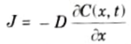
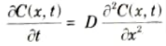
Q5. Write the diffusion equation at any given distance and time.
Ans. The equation of Fick’s first law of diffusion is,
The equation of Fick’s second law of diffusion is,
Q6. Which are the most important contaminants in deep-lying impurities ?
Ans. The most significant contaminants in deep-lying impurities are copper, gold, and iron due to their relatively high solid solubilities in silicon.
Q7. How the liquid source is used in diffusion systems ?
Ans. A carrier gas is bubbled through the liquid in a liquid source before being carried as vapour to the surface of the slices, where it is employed in a diffusion system.
Q8. What do you understand by ion-implantation ?
Ans. Dopant atoms are accelerated, evaporated, and directed at a silicon substrate during ion-implantation.
Q9. What are the advantages of ion-implantation technique?
Ans. Advantages of ion-implantation techniques :
- 1. The profiles have good homogeneity and reproducibility.
- 2. Accurate control of implanted ion dosage using current measurement. Low temperatures were experienced during the process.
- 3. Various materials can be used for masking, e.g., oxide, nitride, metals, and resist.
- 4. Implantation through thin layers, e.g., SiO2 is possible.
Q10. Compare between diffusion and ion-implantation.
Ans.
| S. No. | Diffusion | lon-implantation |
| 1. | It is possible to define diffusion as the movement of contaminants inside a substance. | A low temperature procedure called lon-implantation is used to alter the chemical and physical characteristics of materials. |
| 2. | It done at high temperatures. | It done at low temperatures. |
| 3. | Amount of dopant cannot be controlled. | Amount of dopant can be controlled. |
| 4. | Comparatively less expensive. | More expensive because it require specific equipment. |
Q11. What does ion source contain ?
Ans. lon sources usually consIst of:
- i. Compounds of the desired species.
- ii. A mean for their ionization prior to delivery to the accelerator column.
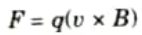
Q12. Write the principle of mass separation.
Ans. The underlying idea is based on the dynamics of charged particles with mass and velocity v travelling perpendicular to a flux density B homogeneous magnetic field. So that, these particles experienced a force such that
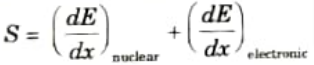
Q13. Define the total stopping power of the target.
Ans. The total stopping power S of the target, defined as the energy (E) loss per unit path length of the ion (x). It is the sum of two terms:
Q14. What are the two key parameters for ion-implants ?
Ans. Two key parameter for ion-implants are:
- i. The ion energy which determines the penetration depth.
- ii. The ion current which sets the dose.
Q15. How the ion beams are produced?
Ans. Typically, ion beams are created in a discharge chamber, where they are contaminated by atomic and molecular ion species that sputter from the chamber’s walls and filaments.
Unit-V: Metallization and Packaging of VLSI Devices (Short Question)
Q1. What is metallization ?
Ans. The technique through which aluminium conductors are used to connect the components of integrated circuits is known as metalization. This procedure creates a thin-film metal layer that will act as the necessary conductor pattern for connecting the different chip components.
Q2. Write the applications of metallization.
Ans. i. Gates and Interconnection: By virtue of the connector runners’ resistance, it regulates the circuit’s speed.
ii. Ohmic contacts: A reliable ohmic contact, which is often created by depositing metal as the semiconductor, does not alter the properties of the device and is stable from an electrical and mechanical standpoint.
Q3. Name the properties of metallization for integrated circuits.
Ans. Properties of metallization for integrated circuit are:
- i. Low resistivity.
- ii. Easy to form.
- iii. Surface smoothness.
- iv. Mechanical stability.
- v. Low stress.
Q4. Why aluminium is preferred for metallization ?
Ans. Aluminium has been the preferred metal because of the following reasons:
- 1. The ease of processing.
- 2. Ability of aluminium to reduce native SiO2 which is always present on silicon wafers exposed to atmosphere.
- 3. It has low resistivity.
Q5. What are the types of deposition process?
Ans. There are two types of deposition process:
- i. Chemical vapor deposition.
- ii. Physical vapor deposition.
Q6. Write the types of physical vapor deposition.
Ans. There are two types of physical vapor deposition
- i. Evaporation.
- ii. Sputtering.
Q7. Explain the process of evaporation method.
Ans. The condensation of the vapour on a substrate that is kept at a lower temperature than the vapour creates a film when using the evaporation method.
Q8. What do you mean by sputtering?
Ans. Any materials, including metals, alloys, semiconductors, and insulators, can be processed using sputtering because it is a very well-controlled technique.
Q9. What is reactive sputtering ?
Ans. Metal can be sputtered in a reactive environment to deposit the chemical. As a result, the sputtering chamber can be used to deposit carbide, nitride, and boride using gases like methane, ammonia or nitrogen, and diborane. This process is known as reactive sputtering.
Q10. Write the problems that are associated with the metallization.
Ans. Various metallization problems are :
- i. Deposition.
- ii. Processing.
- iii Metallurgical and chemical interaction.
- iv. Electromigration.
- v. Device performance.
Q11. Name the different type of IC packages.
Ans. Different types of IC packages are:
- i. DIPS (Dual in packages).
- ii. SIP(Single in package).
- iii. TAB(Tape-automated bonding).
- iv. Bare chips.
Q12. Write all the packaging design considerations.
Ans. Packaging design considerations are:
- i. VISI Design rules,
- ii. Thermal consideration,
- iii. Electrical consideration, and
- iv. Mechanical design consideration.
Q13. Name the two steps for die interconnection ?
Ans. Die interconnection consists of two steps:
- i. The back of the die is mechanically fastened to a suitable mounting medium, such as a metal lead frame, ceramic substrate, or multilayer ceramic package-piece portion.
- ii. The bond pads on the circuit side of the die are electrically interconnected to the package.
Q14. What are the major choices for die-attach process?
Ans. The major choices for a die-attach process are:
- i. Hard solder.
- ii. Polymer.
- iii. Ag-filled glasses.
Q15. How the velocity is controlled in the molten molding compound ?
Ans. To control the velocity of the molten molding compound, each device cavity has a gate or restriction to slow the material flow.
Q16. What is the function of thermoset molding material ?
Ans. Typically, huge multicavity moulds are used to transfer-mold thermoset moulding materials. The warmed moulding compound melts and flows after entering the pot under pressure and heat to fill the mould cavities containing the leadframe strips and the associated ICs.
Q17. How the ball-wedge bonding formed?
Ans. The inside portion of the tip creates the ball bond, while the outer portion of the tip can be used to create the wedge bond anywhere on a 360° area surrounding the ball bond.
Q18. List the basic process for IC fabrication.
Ans.
- 1. Lithography
- 2. Etching
- 3. Deposition
- 4. Chemical Mechanical Polishing
- 5. Oxidation
- 6. Ion-Implantation
- 7. Diffusion
Q19. What is step coverage problem in IC fabrication ?
Ans. i. This happens when a step in an oxide is covered in an abnormally thin layer of resist.
ii. It can result in the resist failing during the etching procedure that follows.
iii. The adoption of planarization techniques helps lessen step coverage issues.

VLSI Technology Btech Quantum PDF, Syllabus, Important Questions
| Label | Link |
|---|---|
| Subject Syllabus | Syllabus |
| Short Questions | Short-question |
| Question paper – 2021-22 | 2021-22 |
VLSI Technology Quantum PDF | AKTU Quantum PDF:
| Quantum Series | Links |
| Quantum -2022-23 | 2022-23 |
AKTU Important Links | Btech Syllabus
| Link Name | Links |
|---|---|
| Btech AKTU Circulars | Links |
| Btech AKTU Syllabus | Links |
| Btech AKTU Student Dashboard | Student Dashboard |
| AKTU RESULT (One VIew) | Student Result |
2 thoughts on “Aktu VLSI Technology KEC-053 Btech Short Question, Quantum Book Pdf”