Table Of Contents
With Aktu Btech Quantum Notes, you can delve into VLSI Technology. Using these important, often asked questions, you can master key topics and excel in your tests. Begin your path to success today! Unit-3 Lithography and Polysilicon Film Deposition
Dudes 🤔.. You want more useful details regarding this subject. Please keep in mind this as well.

Important Questions For VLSI Technology:
*Quantum             *B.tech-Syllabus
*Circulars              *B.tech AKTU RESULT
* Btech 3rd Year   * Aktu Solved Question Paper
Q1. Explain lithography with neat schematic diagram.
Ans. 1. Fig. illustrates schematically the lithographic process used to fabricate circuit chips.
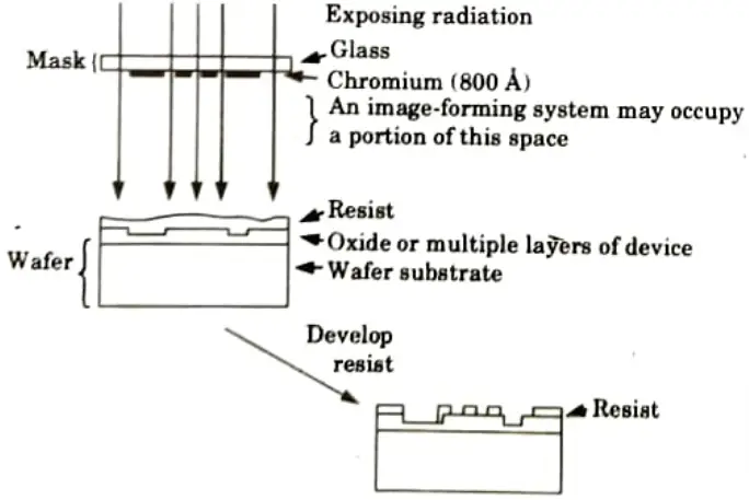
- 2. The “transparent” portions of a mask allow the exposing radiation to pass through.
- 3. Some of the radiation is blocked by the circuit pattern of opaque chromium. A chromium glass mask of this kind is used with ultraviolet (UV) light. Electrons, X-rays, and ions are further forms of electromagnetic radiation.
- 4. Where the distance between the mask and wafer is small, shadow (proximity) printing may be used.
- 5. The process is known as contact printing when there is no gap.
- 6. Another option is to place an image-forming device (like a lens) in between the mask and the wafer.
- 7. As a result, lithography used in the production of integrated circuits is comparable to lithography used in the arts.
- 8. The artist corresponds to the circuit designer. The slabs serve as circuit levels’ masks.
- 9. The press relates to the exposure mechanism, which matches each level to a finished level as well as exposing each level.
- 10. The ink can be compared to either the radiation used to expose the surface or the radiation-sensitive resist. And by employing the resist as a stencil, the paper can stand in for the wafer that will be used to etch the designs.
- 11. Optical lithography has penetrated the “1 𝛍m barrier” of resolution.
- 12. As other lithographic techniques such as those using electron, X-ray, or ion radiation have improved, so has optical lithography.
- 13. For these competing methods large teams of capable people have been working steadily for ten years or more.
- 14. Several methods have only one or two key problems remaining to be solved. Solution generally requires application of standard, but difficult and meticulous, engineering.
Q2. Write a short note on electron lithography.
Ans.
- 1. Due to the 10–50 keV electrons’ short wavelength, electron lithography enables greater resolution than optical lithography.
- 2. Electron diffraction, scattering in the resist, and other aberrations of the electron optics are what restrict the resolution of electron lithography systems, not other factors.
- 3. Commercial systems are already available, and scanning electron-beam systems have been under development for 20 years.
- 4. The best photomask pattern generator has turned out to be the EBES (Electron Beam Exposure System) device. It is commonly utilised in mask stores. The pattern writing is serial, hence throughput is substantially lower than for optical systems.
- 5. Direct wafer patterning has been used for many years to manufacture some specialized devices, such as microwave transistors.
- 6. Some levels were designed optically and others by electron beam in the initial application to low-volume integrated circuits.
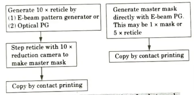
Q3. Explain in detail about the generation of photomask with suitable diagram.
Ans.
- 1. The first use of electron-beam pattern generators has been in photomask making.
- 2. Two approaches to creating a photomask are shown in Fig. An optical pattern generator, which can expose and position pattern elements at a rate of 60 to 100 exposures per minute and is controlled by a computer, is used to pattern a reticle on the left.
- 3. The pattern element is a representation of a variable-sized lighted aperture.
- 4. Next, a step-repeat camera is utilized with the reticle as the object, stepping the reduced image into the appropriate mask area.
- 5. Interferometric regulation of stepping precision. A projection printer or a contact printer may employ the created master mask or copies of it.
- 6. For complicated devices, the main benefit of using an electron-beam pattern generator to create the reticle is speed.
- 7. An optical pattern generator can run for up to 20 hours on a big, dense chip, but an electron-beam pattern generator can run for just two hours or less.
- 8. On the right, Fig. shows the more efficient method of electron beam patterning. The mask may be either a 1 x mask or a 5 x or 10 x reticle for use in a wafer stepper.
Q4. Explain the kinetics of wet etching. How gold is etched?
Ans. A. Wet chemical etching:
- 1. Wet chemical etching of any material can be considered as a sequence of three steps:
- a. Transport of the reactant to the surface.
- b. Reaction at the surface.
- c. Movement of reaction products into the volume of etchant solution.
- 2. As the surface activity is a strong function of localized defects and crystallographic orientation, an etch procedure that is constrained by the rate of surface response will tend to enhance surface roughness and encourage faceting.
- 3. The rate at which the etchant diffuses through a surface-covering, immobile layer can be used to limit etching.
- 4 Generally, for every 10°C increase in temperature, the etch rate doubles.
- 5. Because of this, consideration must be given to these elements when creating an etch process environment for use in a production, in addition to the selection of chemicals and their concentrations.
- 6. The temperature-dependent characteristics of etching can be used to advantage in situations where it is essential to keep residual surface contamination to a minimum.
- 7. In this case, the solution is to operate at a high temperature while using a high dilution of deionized water to maintain a reasonable etch rate.
- 8. Using a cooled etch solution is advised in other circumstances when precise etch control is sought.
- 9. For etching purposes, a variety of chemical chemicals and their combinations are used.
- 10. A lot of these are readily available in “transistor-grade” purity and are chosen to reduce semiconductor contamination during processing.
- 11. All of these reagents naturally contain water. Furthermore, deionized water is always utilised as a diluent.
B.
- 1. Mixtures of nitric acid and hydrochloric acid (in a mixing ratio of 1 : 3 also called aqua regia) are able to etch gold at room temperature.
- 2. The very strong oxidative effect of this mixture stems from the formation of nitrosyl chloride (NOCI) via
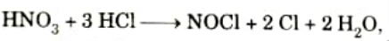
- 3. While free Cl radicals formed in the solution keep the noble metal dissolved as Cl-complex (tetrachloro gold-(III)-acid = HAuCl4). HNO3/HCI mixtures are not stable and decompose accompanied by the formation of nitrogen oxides and Cl2.
- 4. The etch rate of aqua regid for gold is approx. 10 𝛍m/min (at room temperature) and can be increased to several 10 𝛍m/min at elevated temperatures.
Q5. Explain semiconductor etching.
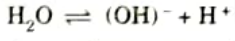
Ans. 1. In semiconductor etching, the primary oxidizing species is (OH)-.Often this is formed by the dissociation of water, which is present in the etchant, as given by
- 2. The production of an oxide prevents the semi-conductor from being further oxidised, necessitating the inclusion of additional chemicals to dissolve it into compounds or complexes that are soluble in water.
- 3. Stirring gets rid of them, allowing for more oxidation to take place on the semiconductor surface.
- 4. A variety of complexing agents can be utilised for this purpose, including bases, acids, and salts with (CN,) and (NH,) groups.
- 5. The availability of high purity reagents and the desire to prevent metallic ion contamination place restrictions on the options available in practical systems.
- 6. For silicon etching systems, hydrofluoric acid is therefore always the best option.
- 7. GaAs systems often use sulfuric, phosphorite, and citric acid, or ammonium hydroxide.
Q6. Explain the structure of polysilicon.
Ans.
- 1. The structure of polysilicon is strongly influenced by dopants, impurities, deposition temperature, and post-deposition heat cycles.
- 2. Polysilicon deposited below 575 °C is amorphous with no detectable structure.
- 3. Polysilicon deposited, above 625 °Cis polycrystalline and has a columnar structure.
- 4. Crystallization and grain growth occur when either amorphous or columnar polysilicon is heated.
- 5. Amorphous or columnar polysilicon does not significantly vary structurally during high-temperature heat cycles.
- 6. Although numerous factors, including deposition rate, partial hydrogen pressure, total pressure, the presence of dopants, and the presence of impurities, affect the deposition temperature at which the transition from amorphous to columnar structure occurs, it is well defined (O, N, or C).
- 7. The transition temperature for depositions in an LPCVD reactor is between 575 and 625 °C.
- 8. Polysilicon recrystallizes when heated after deposition, although the temperature at which this occurs is greatly controlled by the dopants and impurities.
- 9. At temperatures exceeding 1000°C, oxygen, nitrogen, and carbon impurities help to maintain the amorphous structure.

VLSI Technology Btech Quantum PDF, Syllabus, Important Questions
| Label | Link |
|---|---|
| Subject Syllabus | Syllabus |
| Short Questions | Short-question |
| Question paper – 2021-22 | 2021-22 |
VLSI Technology Quantum PDF | AKTU Quantum PDF:
| Quantum Series | Links |
| Quantum -2022-23 | 2022-23 |
AKTU Important Links | Btech Syllabus
| Link Name | Links |
|---|---|
| Btech AKTU Circulars | Links |
| Btech AKTU Syllabus | Links |
| Btech AKTU Student Dashboard | Student Dashboard |
| AKTU RESULT (One VIew) | Student Result |