Explore VLSI Technology with Aktu Btech Quantum Notes. Use these important, commonly asked questions to master key concepts and thrive in tests. Begin your journey to prosperity right now! Unit-2 Epitaxy and Oxidation
Dudes 🤔.. You want more useful details regarding this subject. Please keep in mind this as well.

Important Questions For VLSI Technology:
*Quantum             *B.tech-Syllabus
*Circulars              *B.tech AKTU RESULT
* Btech 3rd Year   * Aktu Solved Question Paper
Q1. What is epitaxial growth ? What are the advantages of epitaxial process over diffusion and Czochralski process ?
Ans. A. Epitaxial growth: A thin crystalline layer is grown on a crystalline surface via the technique known as epitaxial growth (substrate). As a seed crystal, the substrate wafer is used. By using an evaporation technique, crystal is created in this process below the melting point.
B. Advantage of epitaxial process over diffusion process:
- 1. Device engineers can regulate the doping profiles with the epitaxial process, which is not possible with the diffusion method.
- 2. Using the epitaxial method, the physical and chemical characteristics of the wafer can be altered.
C. Advantage of epitaxial process over Czochraleki process:
- 1. Unlike the Czochralski process, crystalline thin films can be grown below the melting point using epitaxial process.
Q2. Describe dopant profile in brief.
Ans.
- 1. The same factors that the growth process takes into account apply when incorporating dopant atoms into the epitaxial layer.
- 2. The source of the dopant is the hydrides of the impurity atoms.
- 3. Because there is a lot of hydrogen present in the process, thermodynamic calculations show that the hydrides are rather stable.
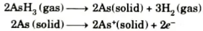
- 4. Arsine is being absorbed on the surface, decomposed, and being incorporated into the growing layer.
- 5. The doping process and the growth process interact with one another.
- 6. The creation of these species’ chlorides is a competitive process in the cases of boron and arsenic.
- 7. The amount of dopant integrated into the silicon depends on the growing rate of the film.
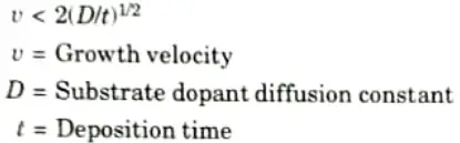
- 8. Equilibrium between the solid and gas phases is created at low growth rates, however it is not attained at larger growth rates.
- 9. Solid-state diffusion and evaporation are used to liberate the dopant from the substrate.
- 10. Either at the interface or through gas phase diffusion, this dopant is reincorporated into the developing layer.
Q3. Explain auto doping process.
Ans.
- 1. It is manifested as an enhanced transition region between the layer and the substrate.
- 2. The shape of doping profile, close to the substrate, is dominated by solid-state diffusion from the substrate and is a complementary error function if
- 3. Auto doping is a phenomenon that changes with time. By use of solid state diffusion, the dopant that evaporates from the wafer interior is fed to the wafer surface.
- 4. As a result, with time, the flux of dopant from an exposed surface declines and is not constant.
- 5. As the purposeful doping takes over and the auto doping is reduced, the profile becomes flat.
- 6. The substrate dopant species, as well as reaction variables like temperature and growth rate, influence the size of the auto doping tail.
- 7. Both the minimum doping level and the minimum layer thickness that can be developed with controlled doping are constrained by auto doping.
Q4. Write short notes on chemical vapor deposition (CVD).
Ans.
- 1. Typically, a reactor made of an elemental quartz reaction chamber and a susceptor is used to execute chemical vapour deposition (CVD) of single crystal silicon.
- 2. The susceptor gives the material wafer physical support and creates a more consistent heat environment.
- 3. As process gases enter the chamber, deposition takes place at a high temperature where various chemical reactions happen.
Q5. What is Epitaxy ? Discuss Molecular Beam Epitaxy technique in brief. What are the advantages of MBE over VPE ?
Ans. A. Epitaxy: A thin crystalline layer is grown on a crystalline surface via the technique known as epitaxial growth (substrate). As a seed crystal, the substrate wafer is used. By using an evaporation technique, crystal is created in this process below the melting point.
B. Molecular Beam Epitaxy:
- 1. Fig. shows a simple schematic illustrating the basic principle of MBE.
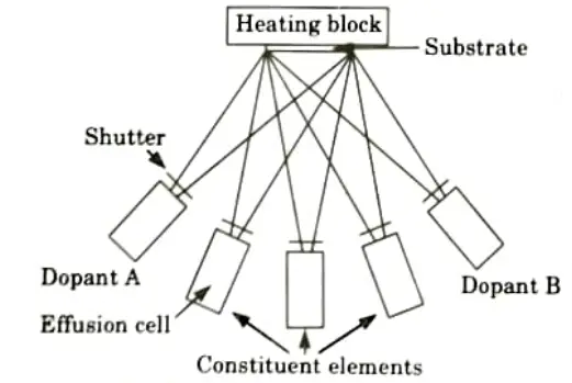
- 2. In Molecular Beam Epitaxy (MBE), the material to be produced or its constituent parts are directly transported physically to a heated substrate.
- 3. Growth is consequently done by directing atomic or molecular beams in a well-controlled, ultra-high-vacuum system, and is fundamentally comparable to vacuum evaporation.
- 4. MBE can be used to generate silicon as well as GaAs.
- 5. The raw materials for GaAs are gallium and arsenic. Moreover, layers of AlGaAs are grown using aluminium.
- 6. To create silicon and SiGe alloys, elemental silicon and germanium are used.
- 7. Thermal evaporation from crucibles known as effusion cells, which are shuttered to start and stop the flux of the evaporant species, often produces the beams of material to be carried.
- 8. A number of effusion cells are arranged so that their flux is directed towards the substrate, each with a separate shutter.
- 9. Thermal evaporation is employed for germanium, while electron beam heating is frequently used in the case of silicon MBE to produce a sizable flux of source material.
- 10. To improve layer uniformity, the substrate on which the wafer is placed is often made of a heated molybdenum block that may be rotated slightly during growth.
- 11. Sample mounting is done by means of indium or gallium on its back face or by means oft mechanical fasteners.
C. Advantages of MBE over VPE:
- 1. MBE is low temperature process which is advantageous for VLSI
- 2. While preparing thin layers using MBE process, autodoping and autodiffusion both are minimized.
- 3. The MBE process can be used for generating complicated doping profiles as it regulates the amount of dopant.
- 4. As MBE process is based on the evaporation of silicon and the dopants, hence no chemical reactions are involved in it.
Q6. What is latch up ? How latch up is avoided in CMOS technology?
Ans. i. Latch up:
- 1. Latch up refers to short circuit formed between power and ground rails in an IC leading to high current and damage to the IC.
- 2. In CMOS transistor, latch up is the phenomenon of low impedance path between power rail and ground rail due to interaction between parasitic pnp and npn transistors.
ii. Latch up avoided in CMOS technology:
- 1. It is possible to design chips to be resistant to lateh-up by adding a layer of insulating oxide that surround both the NMOS and the PMOS transistors. This breaks the parasitic silicon-controlled rectifier (SCR) structure between these transistors.
- 2. Devices fabricated in lightly doped epitaxial layers grown on heavily doped substrates are also less susceptible to latch-up.
- 3. Also to avoid the latch, a separate tap connection is put for each transistor.

VLSI Technology Btech Quantum PDF, Syllabus, Important Questions
| Label | Link |
|---|---|
| Subject Syllabus | Syllabus |
| Short Questions | Short-question |
| Question paper – 2021-22 | 2021-22 |
VLSI Technology Quantum PDF | AKTU Quantum PDF:
| Quantum Series | Links |
| Quantum -2022-23 | 2022-23 |
AKTU Important Links | Btech Syllabus
| Link Name | Links |
|---|---|
| Btech AKTU Circulars | Links |
| Btech AKTU Syllabus | Links |
| Btech AKTU Student Dashboard | Student Dashboard |
| AKTU RESULT (One VIew) | Student Result |