
With our AKTU question paper and solution, you can discover the wonders of VLSI Technology. Explore into quantum notes, where you’ll learn about amazing concepts in a fun and engaging approach for young minds.
Dudes 🤔.. You want more useful details regarding this subject. Please keep in mind this as well.

Important Questions For VLSI Technology:
*Quantum          *B.tech-Syllabus
*Circulars           *B.tech AKTU RESULT
* Btech 3rd Year
Section A: VLSI Technology Question with Short Answers
a. Discuss oxide charges.
Ans. Four different types of charge identified in thermally grown oxide on a silicon surface.
- i. Interface trapped charge:
- 1. The interface trapped charge density Qit interface states exists at the Si/SiO interface.
- 2. Defects at the interface generate charge traps or electronic energy levels with energy states (E) in the silicon bandgap, which can capture or emit mobile carriers.
- ii. Fixed oxide charge: The fixed charge density Qf is the immobile charge always present and located within 1 nm transition layer of nonstoichiometric silicon oxide (SiOx) at the boundary between the silicon and SiOs layer.
- iii. Oxide trapped charge: The oxide trapped charge density Qot is associated with the defects in SiO2Qot is located in traps distributed throughout the oxide layer.
b. What is electronic grade silicon ?
Ans. Electronic-Grade Silicon (EGS), a high-purity polycrystalline material, is the starting point for the production of single-crystal silicon. Without a doubt, EGS is one of the purest materials accessible. Boron, carbon, and residual donors are the main contaminants.
c. Explain the purpose of oxidation.
Ans.
- 1. To serve as a mask against implant or diffusion of dopant into silicon.
- 2. To provide surface passivation.
- 3. Ability to form a high quality oxide in a controlled and preferable manner.
d. How is wafer polishing done ?
Ans. Chemical mechanical polishing (CMP) is used in the polishing industry lo polish silicon wafer.
e. What are positive and negative photoresist ?
Ans.
| S. No. | Positive photoresist | Negative photoresist |
| 1. | The exposed areas are soluble. | The exposed areas are insoluble for wet chemical development. |
| 2. | It has more expensive. | It has less expensive. |
| 3. | It has bad resistance in etching or implantation process. | It has excellent resistance against etch or implantation processes. |
f. What are the disadvantages of Electron Beam Lithography?
Ans. Disadvantages of electron beam lithography are:
- i. High system cost.
- ii. System complexity due to requirement of vacuum.
g. What are the basic mechanisms of diffusion?
Ans. Diffusion can occur by two different mechanisms:
- i. Interstitial diffusion: Substitutional diffusion happens when atoms shift from one atomic location to another.
- ii. Substitutional diffusion: In this situation, the diffusing atom is on an interstice rather than a lattice site. Unless it is already occupied, the diffusing atom is free to travel to any adjacent interstice.
h. State Fick’s second law of diffusion.
Ans.
- 1 Fick’s second law may be derived by applying considerations of continuity.
- 2. Consider the flow of particles in a crystal of cross section A, between planes P1 and P2 separated by dx, as shown in Fig.
- 3. The rate of accumulation of particles in the region between planes is
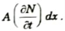
- 4. This can also be written as the difference between the fluxes flowing into and out of the region.
- 5. The flux entering the region at P1 is Aj, and the flux leaving the region at P2 is A(j+dj). The net flux entering the region is thus -A dj.
Hence,
- 7. Eq. (4.7.2) involves only measurable quantities such as volume concentration, diffusion depth and diffusion time.
i. Why is metallization done?
Ans. Metallization establishes a barrier between the underlying structure and the elements, which can extend the building’s lifespan and retain its beauty. Lower maintenance costs-painted surfaces will need to be repainted on a regular basis to maintain the finish.
j. What is the disadvantage of sputtering ?
Ans. Disadvantages of sputtering:
- i. Sputtering rates are low in comparison to those achievable through thermal evaporation.
- ii. Sputtering targets are frequently expensive, and material utilization may be poor.
- iii. The majority of the energy impacting on the target is converted to heat, which must be eliminated.
- iv. To avoid poisoning the sputtering target, the gas composition in reactive sputter deposition must be carefully regulated.
Section B: VLSI Technology Important Question with Solution
a. Explain Czocharlaski method of single crystal generation in detail.
Ans.
- 1. The concept of a CZ system for both silicon and GaAs crystal formation is shown in Fig. The melt is confined in a tumble and accepted in a molten state by heating.
- 2. A seed crystal suitably oriented, is suspended over the crucible in a chuck. For growth the seed is inserted into the melt until its end is molten.
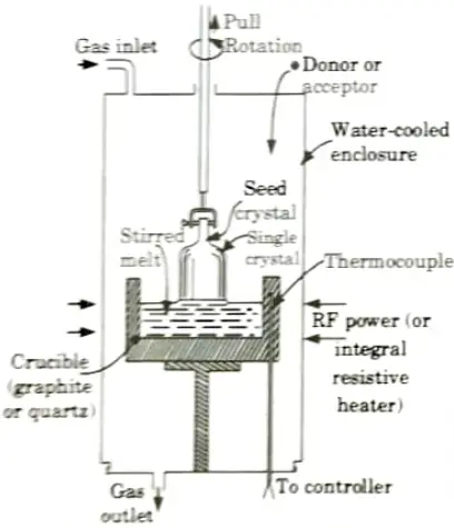
- 3. It is presently being gradually phased out. As a result, a single crystal forms at the liquid-solid boundary through gradual freezing. Pull rates of 50-100 mm/hr are normal for silicon and GaAs.
- 4. Accommodations are also made during the pulling operation to rotate the crystal, and sometimes the crucible as well.
- 5. To manage radial temperature gradients during the solidification process, a series of annular heat shields are installed between the growing region and the reactor walls.
- 6. For silicon, the complete assembly is sealed within a water-cooled envelope that is flushed with an inert gas.
- 7. In the case of GaAs, it is critical to maintain an arsenic overpressure of around 1.0 atm to prevent melt breakdown during crystal formation.
- 8. During the development process, the latent heat of fusion must be eliminated from the crystal-melt system. This heat is dissipated through thermal conduction along the crystal axis and radiation from the crystal surface.
b. Explain Plasma Oxidation technique for the growth of wide layer.
Ans.
- 1. The anodic plasma-oxidation process allows for the development of high-quality techniques.
- 2. This technique has all of the advantages associated with low temperature processing, such as reduced movement of prior diffusions and defect formation suppression.
- 3. At low temperatures, anodic plasma oxidation can produce reasonably thick oxides.
- 4. Plasma oxidation is a low-temperature vacuum process that is often performed in pure oxygen discharge.
- 5. The plasma is generated by either a high-frequency discharge or a direct current electron source.
- 6. The rate of oxide development normally rises with increasing substrate temperature, plasma density, and dopant concentration in the substrate.
c. Explain Chemical Vapor Deposition process.
Ans.
- 1. Chemical vapour deposition (CVD) of single crystal silicon is typically conducted in a reactor comprised of an elemental quartz reaction chamber including a susceptor.
- 2. The susceptor supports the material wafer physically and creates a more homogeneous temperature environment.
- 3. Deposition takes place at a high temperature, where many chemical reactions occur when process gases flow into the chamber.
d. What are the disadvantages of using Aluminum for metallization ? How are they rectified ?
Ans. Disadvantages of using aluminum for are:
- 1. If the temperature rises beyond 600 °C during packing, or if there is overheating due to a current spike, Al can fuse and penetrate through the oxide to the silicon, causing a short circuit in the connection. Such failures can be reduced by providing proper process control and testing.
- 2. Purple plague is one of six possible phases that might arise when gold and aluminium interact. Due to the different rates of diffusion of gold and aluminium, voids typically appear in the form of the purple plague. These holes can cause weak bonding, resistive bonds, or catastrophic collapse. In circuits that will be subjected to high temperatures, the problem is typically remedied by employing aluminium lead wire or another metal system.
- 3. Aluminium suffers from electromigration which can cause considerable material transport in metals. It occurs because of the enhanced and directional mobility of atoms caused by the direct influence of the electric field and the collision of electrons with atoms, which leads to momentum transfer. In thin-film conductors that carry sufficient current density during device operations, the mode of material transport can occur at much lower temperature because of the presence of gain boundaries, dislocations and point defects that aid the material transport.
Section 3: RCA Cleaning
a. Explain Float-Zone method of single crystal generation.
Ans.
- 1. Container less floating zone crystal formation is a process for purifying crystals and alloys. The basic layout of this technique is depicted in Fig.
- 2. Because no crucible is necessary in this procedure, contamination from the container can be avoided.
- 3. However, the size and quality of crystals generated by this process are limited by the earth’s gravity.
- 4. Access to a low-gravity environment aboard a spaceship gives up new opportunities for container less processing because gravity and natural convection (two of the hypothesized main drivers of crystal defects on Earth) are minimized in space.
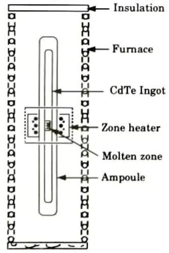
- 5. The floating zone (FZ) technique is a crucible-free crystal growth method. In FZ growth, the molten zone is kept between two vertical solid rods by its own surface tension as shown in Fig.
- 6. To grow a single crystal, dip a seed crystal into one end of the zone and translate the molten zone towards the feed stock.
- 7. The fundamental advantage of the FZ technique is the lack of a container, which eliminates crucible material contamination and the production of crystal defects induced by the contact of the growing crystal and the container.
- 8. As a result, the approach is particularly applicable to highly reactive materials, intermetallic complexes, and refractory materials. The molten zone can be heated by a variety of means, including RP induction, optical, electron beam, laser, and resistance heating.
b. Demonstrate RCA cleaning with analysis of all steps and chemicals.
Ans. A. Objective of wafer cleaning: The removal of particle and chemical contaminants from the semiconductor surface without hurting or negatively affecting the substrate surface is the goal of wafer cleaning.
B. RCA:
- 1. One highly successful approach to cleaning silicon, known as “RCA clean, is to use two solutions in sequence.
- 2. The first of these consists of 1:1:5 to 1:2:7 volumes of NH4OH: H2O2:HO2.
- 3. Here, the H2O2 functions to oxidize all remaining organic contaminants on the surface, which are present because of incomplete removal of photoresist, and also because of airborn materials and physical handling.
- 4. The NH4OH is effective in removing heavy metals such as cadmium, cobalt, copper, iron, mercury, nickel, and silver by forming amino complexes with them.
- 5. Next, a solution consisting of HCl: H2O2: H2O in a 1:1:6 to 1:2:8 volume ratio is used to remove aluminum, magnesium, and the light alkali ions, and to prevent displacement replating from the solution.
- 6. Each of these steps is carried out for 10-20 min at 75-85°C, under conditions of rapid agitation. Nitrogen gas bubbling through the etchants is often used for this purpose.
- 7 Finally, wafers are blown dry and stored in a clean environment until further processing.
- 8. Results with this cleaning technique make it quite suitable for bipolar as well as MOS microcircuits, so that it is in wide use in industry at the present time.
Section 4: Molecular Beam Epitaxy
a. Explain molecular beam epitaxy process in detail. Also write the advantages and disadvantages of this method.
Ans. A. Molecular beam epitaxy and advantages:
- 1. Fig. shows a simple schematic illustrating the basic principle of MBE.
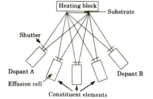
- 2. Molecular beam epitaxy (MBE) is the direct physical transport of a substance or its components to a heated substrate.
- 3. In essence, it is comparable to vacuum evaporation, with growth performed by directing atomic or molecular beams in a well-controlled, ultra-high-vacuum system.
- 4. MBE can generate silicon as well as GaAs.
- 5. Gallium and arsenic are employed as GaAs source materials. Aluminum is also employed in the formation of AlGaAs layers.
- 6. Silicon and SiGe alloys are manufactured using the elements silicon and germanium.
- 7. Material beams are often formed by thermal evaporation from crucibles known as effusion cells, which are shuttered to commence and end the flux of evaporant species.
- 8. A sequence of effusion cells, each with its own shutter, are arranged in such a way that their flux is directed to the substrate.
- 9. However, in the case of silicon MBE, electron beam heating is frequently utilised to generate a substantial flow of source material, whereas thermal evaporation is used for germanium.
- 10. The substrate on which the wafer is mounted is typically a heated molybdenum block that may be moved at a few rpm during growth to improve layer uniformity.
- 11. Sample mounting is done by means of indium or gallium on its back face or by means oft mechanical fasteners.
B. Disadvantages of MBE Process:
- 1. For overall perfect and pure film, it is necessary low to maintain a very pressure of the order of 10-10 Torr which is slightly difficult.
- 2. This process is very expensive as compared to CVD process.
- 3. The growth rate in MBE process is 0.01-0.3 𝛍m/min which is very small compared to the growth rate of 1 𝛍m/min in CVD process.
b. Explain Deal-Grove’s model for oxidation kinetics.
Ans. A. Reason: Oxidation is done in a regulated and repeatable manner to produce high quality oxide. This mechanism acts as a shield against dopant implant or diffusion into silicon, as well as providing surface passivation.
B. Deal-Grove’s model:
- 1. Deal and Grove’s model describes the kinetics of silicon oxidation.
- 2. The model is generally valid for temperatures between 700 and 1300 °C, partial pressures between 0.2 and 1.0 atm, and oxide thicknesses between 300 and 20,000 A for oxygen and water ambient.
- 3. Fig. shows the silicon substrate covered by an oxide layer that is in contact with the gas phase.
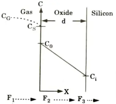
4. The oxidizing species:
i. are transported from the bulk of the gas phase to the gas-oxide interface with flux F1.
ii. are transported across the existing oxide toward the silicon with flux F2 and
iii. react at the Si-SiO2 interface with the silicon with flux F3.
5. For steady state, F1 = F, = F3. The gas-phase flux F1 can be linearly approximated by assuming that the flux of oxidant from the bulk of the gas phase to the gas-oxide interface is proportional to the difference between the oxidant concentration in the bulk of the gas CG and the oxidant concentration adjacent to the oxide surface CS.
F1 = hG(CG-CS)
where KG is the gas-phase mass transfer coefficient.
6. To relate the equilibrium oxidizing species concentration in the oxide to that in the gas phase. we have henry’s law,
7. Using Henry’s law along with the ideal gas law:
8. Ozidation is a non-equilibrium process with the driving force being the deviation of concentration from equilibrium.
9. The fx of this oxidizng species across the oxide is taken to follow Fick’s lew at any point d in the oxide layer.
10. Following the steady-state assumption, F2 must be the same at any point within the oxide, resulting in
where D is the diffusion coefficient,
Ci is the oxidizing species concentration in the oxide adjacent to the oxide silicon interface, and
do is the oxide thickness.
11. Assuming that the flux corresponding to the Si-SiO2 interface reaction proportional to Ci.
F3 = ksCi
where ks is the rate constant of chemical surface reaction for silicon radiation.
Section 5: Electron Beam Lithography
a. Explain the process of electron beam lithography. Write down figures of merit of lithographic process.
Ans. A. Electron beam lithography:
- 1. Because of the short wavelength of the 10-50 keV electrons, electron lithography provides greater resolution than optical lithography.
- 2. Electron diffraction, scattering in the resist, and other aberrations of the electron optics limit the resolution of electron lithography devices.
- 3. For the past two decades, scanning electron-beam systems have been in development, and commercial systems are now available.
- 4. The greatest photomask pattern generator is the EBES (Electron Beam Exposure System) machine. It is commonly seen in mask shops. Because of the serial nature of pattern writing, throughput is significantly lower than with optical systems.
- 5. Nonetheless, some specialised devices, like as microwave transistors, have been made through direct wafer patterning for many years.
- 6. In the first application to low-volume integrated circuits, some levels were patterned optically, while others were patterned with an electron beam.
B. Figure of merit of lithographic process:
- 1. Often, the success of a lithographic process is judged against specific figures of merit or performance indicators.
- 2. The key figure of merit for a lithographic system is picture resolution.
- 3. The photomask must be precisely aligned to the pre-existing layers on the wafer, making overlay the second crucial figure of merit for lithography.
- 4. The third and last figure of merit for a lithographic system is throughput.
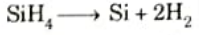
b. Explain the process of polysilicon film deposition.
Ans.
- 1. Polysilicon is used as the gate electrode in MOS devices. A metal or metal silicide, such as tungsten or tantalum silicide, may be deposited over the polysilicon gate to increase the electrical conductivity.
- 2. Polysilicon is also used for resistors, conductors, and to ensure ohmic contact to shallow junctions.
- 3. The polysilocon is deposited by pyrolyzing silane between 575 and 650 °C in a low-pressure reactor. The chemical reaction is
- 4. Further procesSing for polysilicon gates involves doping, etching, and oxidation.
- 5. Two low-pressure processes are common for depositing polysilicon.
- 6. One uses 100 % silane at a pressure of 25 to 130 Pa (0.2 to 1.0 Torr).
- 7. The other process is performed at the same total pressure but uses 20 too 30 % silane diluted in nitrogen.
- 8. Both processes deposit polysilicon on 10 to 200 wafers per run with thickness uniformities of ± 5 %. The deposition rates are 10 to 20 nm/min.
Section 6: Ion-Implantation Process
a. Determine total doping concentration, junction depth and doping profile in case of infinite source of diffusion.
Ans.
- 1. In many cases we are interested in determining the distribution of a diffusing impurity whose initial concentration, C(x, 0), in the silicon is zero.
- 2. The diffusion profile will depend upon the initial and boundary conditions.
- 3. When the diffusion coefficient is constant the diffusion equation in one dimension is
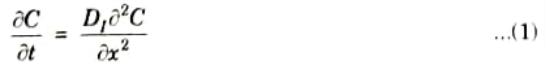
- 4. The solution to eq. (1) when an infinite doping source maintains the surface concentration constant such that C(0, t) = Cs is
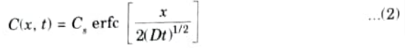
where “ertfc” is the complementary error function.
- 5. The total diffusivity is often obtained by fitting eq. (2) to an experimental diffusion profile.
- 6. This approach is satisfactory for determining the sum of intrinsic diffusivities, DI.
7. But at higher concentrations where DI = DI(C), eq. (2) will only yield an “effective” diffusivity. - 8. For the case where a thin uniformly doped region at the silicon surface is used as a doping source, the initial impurity distribution can be approximated by a constant concentration, C0, Over a distance 𝝳 which gives a concentration per unit area of Q= C0𝝳.
- 9. When eq. (1) is solved under this boundary condition, the resulting Gaussian diffusion profile is given by,
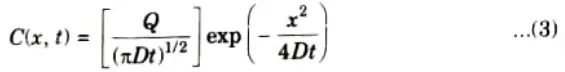
- 10. As the diffusion proceeds the surface concentration decreases with time as
- 11. If the background doping of the silicon is Cb, then the depth at which the indiffusing dopant concentration equals Cb (junction depth)
b. Explain Ion-Implantation process, its advantages and disadvantages.
Ans. A. Ion-Implantation process:
- 1. Dopant atoms are evaporated, accelerated, and directed at a silicon substrate during ion-implantation.
- 2. They penetrate the crystal lattice, impact with silicon atoms, and lose energy gradually before coming to rest at some depth within the lattice.
- 3. The acceleration energy can be adjusted to manage the average depth.
- 4. By monitoring the ion current during implantation, the dopant dose can be adjusted.
- 5. Further heat treatments remove the main side effect, which is the disruption of the silicon lattice caused by ion collisions.
- 6. lon-implantation therefore satisfies the conditions for a generally useful doping process.
- 7. Implantation energies range from 1 keV to 1 MeV, resulting in ion distributions with average depths ranging from 100 A to 10 𝝁m.
B. Advantages:
- 1. Short process times. good homogeneity and reproducibility of the profiles.
- 2. Exact control of the amount of implanted ions by measuring the current.
- 3. Relatively low temperatures during the process.
- 4. Various materials can be used for masking. e.g., oxide, nitride, metals, and resist.
- 5. Implantation through thin layers, e.g. SiO2 is possible.
- 6. Low penetration depth of the implanted ions.
C. Disadvantages:
- 1. Not all the damage can be corrected by annealing.
- 2. Typically has higher impurity content than does diffusion.
- 3. Often uses extremely toxic gas sources such as arsine (AsH3), and phosphine (PH3).
Section 7: CMOS Fabrication
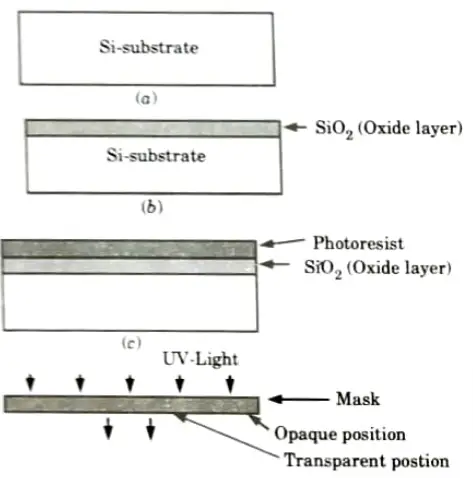
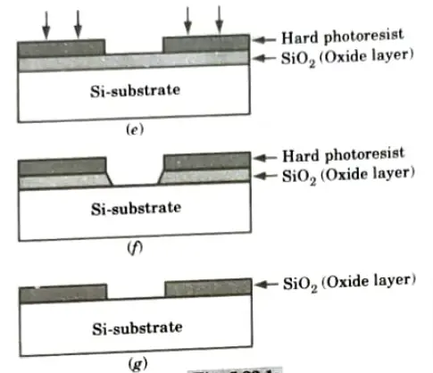
a. Explain CMOS fabrication steps in detail.
Ans.
- 1. The fabrication process involved a set of patterned layers of doped silicon, polysilicon, metal and insulating silicon dioxide.
- 2. Initially silicon substrate has to be taken as shown in Fig.(a).
- 3. The sequence starts with the thermal oxidation of the silicon surface, results in growth of about 1 mm thickness of SiO2 layer as shown in Fig.(b).
- 4. The entire layer is coated with the substance called photoresist, which is a light sensitive, acid-resist organic polymer as shown in Fig.(c).
- 5. When photoresist material is exposed to UV light the exposed portion become soft so that solvents can easily etch that portion.
- 6. To select the specified position for exposure we use mask, it allows the passage of UV light from its transparent portion as shown in Fig.(d).
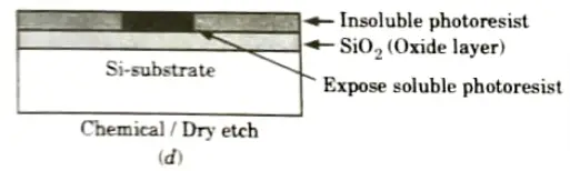
- 7. The type of photoresist initially hard in nature but when exposed to light becomes soft are known as positive photoresist.
- 8. Following the UV exposure step. the soft portion is etched off using solvents (HF acid) as shown in Fig.(e).
- 9. Now, the SiO2 region which is not covered can be etched away by using chemical solvents shown in Fig.(f).
- 10. We obtain an oxide window that reaches down to the silicon surface, the remaining photoresist can now be stripped from rest of SiO2 surface by using another solvents as shown in Fig.(g).
- 11. The sequence of fabrication step actually is a single pattern transfer on to the SiO2 surface.
- 12. The fabrication of semiconductor devices requires several such pattern transfer to be performed on SiO2 polysilicon and metal.
b. Briefly explain vacuum deposition and sputtering for metallization.
Ans. A. Vacuum deposition:
- 1. The arrangement of metallization process using vacuum deposition technique is shown in Fig.
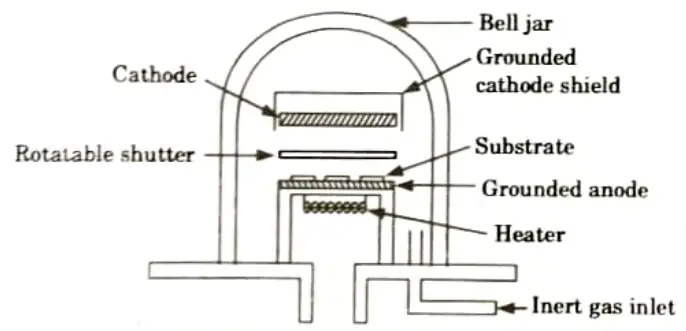
- 2. The silicon wafers are placed face down around the bell jar, with the source of metal in the centre.
- 3. The vacuum pressure is lowered to below 5 x 10⁻⁶ Torr before the metal deposition commences.
- 4. The silicon is then heated to a temperature range of 100 to 300°C, which causes the deposited metal to chemically react with the silicon dioxide and adhere to the wafer surface.
- 5. Upward evaporation is also used to prevent impurities, which may be generated by the heat source, from falling onto the wafers.
- 6. The metal film is normally of 1 𝝁m thickness. The thickness can be monitored by including a quartz crystal oscillator in the vacuum. whose frequency can be set with the amount of metal to be deposited on its surface.
- 7. After evaporation, the wafers are heated at about 1500°C in an inert gaseous (e.g., nitrogen) atmosphere. This causes the metal to alloy well with the silicon surface so that low resistance is achieved in the interface between the two. This is referred to as a low ohmic contact joint.
B. Sputtering:
- 1. In sputter deposition, the target material is blasted with intense ions, causing some atoms to be released. These atoms are then condensed to create a film on the substrate.
- 2. Sputtering methods are highly regulated and can be applied to a wide range of materials, including metals, alloys, semiconductors, and insulators.
- 3. To deposition metal, radio frequency, DC, and DC-magnetron sputtering can be utilised. Because the composition of the film is tied to the composition of the target, alloy-film deposition by sputtering from an along target is achievable.
- 4. This is true even when the sputtering rates of the alloy components differ significantly.
- 5. During the early phases of sputtering, the component with the highest sputtering rate is sputtered preferentially off the target, leaving the target surface deficient in this component.
- 6. The deficient region quickly becomes deficient enough to compensate for the increased sputtering rate, resulting in deposits with a composition comparable to the target.
- 7. The difference in target and film compositions is determined by the type of equipment, sputtering parameters, and alloy constituent.
- 8. Using the right equipment and sputtering conditions, multiple complicated alloys with identical compositions were deposited in the target and the film.
- 9. Alloys can also be deposited with great composition control using individual component targets.
- 10. The compounds can be deposited in some situations by sputtering the metal in a reactive environment.
- 11. Consequently, in the sputtering chamber, gases such as methane, ammonia or nitrogen, and diborane can be utilised to deposit carbide, nitride, and boride, respectively. This is known as reactive sputtering.
5 thoughts on “VLSI Technology: Aktu Important Questions with Solutions and Notes”