With Aktu Btech Quantum Notes, you can enter the world of Integrated Circuits. Master important concepts and ace tests with these frequently asked questions. Access them immediately for success! Unit-5 Integrated Circuit Timer
Dudes 🤔.. You want more useful details regarding this subject. Please keep in mind this as well.

Important Questions For Integrated Circuits:
*Quantum               *B.tech-Syllabus
*Circulars                *B.tech AKTU RESULT
* Btech 3rd Year    * Aktu Solved Question Paper
Q1. Draw the pin-diagram of IC 555 and explain the function of each pin.
Ans. 1. Fig. shows the pin-diagram of 8-pin DIP 555 timer.
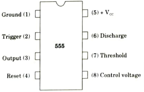
Function:
- 1. Ground: All the voltages are measured with respect to this terminal.
- 2. Trigger: The output of the timer is controlled by this pin. The output is low if the voltage is greater than 2/3 VCC. Por negative going pulse of amplitude larger than 1/3 VCC is applied to this pin, the comparator II output goes high, which in turn makes the output high as long as the trigger terminal has a low voltage.
- 3. Output: The complementary signal out of the flip-flop goes through an output stage and becomes the output of the timer.
- 4. Reset: This pin is connected to supply i.e., +VCC in order to avoid any false triggering. Generally pin 4 is not used.
- 5. Supply +VCC: The 555 times works with supply voltage +5 V to +18 V with respect to ground.
- 6. Discharge: A capacitor is connected externally to the ground at this pin. Internally the collector of the discharge transistor is coming at this pin. A high Q output from the flip-flop makes the transistor OFF, i.e. open circuit and external capacitor charges at a rate determined by external RC network. When output Q is low, transistor gets saturated and external capacitor discharges.
- 7. Threshold: When voltage is greater than or equal to 2/3 VCC the output of comparator I goes high which makes the output of the timer low.
- 8. Control voltage: The pulse width of output waveform can be varied by imposing a voltage at this pin. In most applications this pin is not required and a capacitor is connected to this pin and ground to prevent noise introduction in the circuit.
Q2. What are different modes of operation of IC 555 ? Draw the circuit diagram of a delay circuit using 565. What is maximum delay that can be provided with 555 with a capacitor of 1000 𝝻F?
Ans. A. Modes of operation of IC 555: The timer (555) can operate in two modes:
- i. A monostable (one-shot) multivibrator.
- ii. An astable (free running) multivibrator.
B. Circuit diagram:
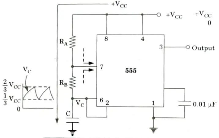
C. Numerical:
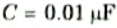
Given: C 1000 𝝻F
To Find: Maximum delay.
1. The total period of output waveform is
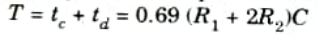
2. For maximum delay, it is given that
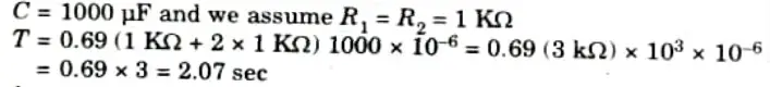
So, the maximum delay is 2.07 seconds.
Q3. Design a 555 timer as astable multivibrator giving its block diagram which provides an output signal frequency of 2 KHz and 75 duty cycle.
Ans. Given: Frequency, fc = 2 KHz, Duty cycle, D = 75 %
To Design: 555 timer as an astable multivibrator.
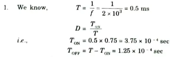
2. Duty cycle is more than 50 % hence modified circuit must be used.
3. The modified circuit is shown in Fig.
4. Let
The charging of C takes place through R1 and diode D while discharging takes place through R2 only
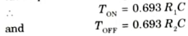
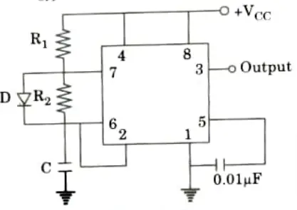
5. Using values of TON, TOFF and C,
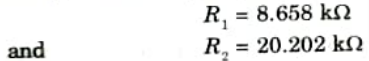
Q4. Explain the operation of VCO with help of functional block diagram. Also show the pin-diagram of VCO.
Ans.
- 1. The pin configuration and the basic block diagram of IC 566 VCO are shown in the Fig.(a) and (b) respectively. The frequency of oscillation is determined by an externally connected resistor R1 and a capacitor C1.
- 2. The control voltage or the modulating input vc is applied at the control terminal (pin 5).
- 3. The triangular voltage obtained at pin 4 is shown in Fig.(c). It is generated by alternately charging the capacitor C1 by one current source, and discharging it linearly through another current source. The amount of charge and discharge voltage swing is determined by the Schmitt trigger.
- 4. The Schmitt trigger also provides the square-wave output at pin 3 through the power amplifier A3 and the triangular output is available at pin 4 through the buffer amplifier A1.
Operation of VCO:
- 1. The output voltage swing of the Schmitt trigger is set to the levels VCC and 0.5VCC. In Fig. if Ra = Rb in the positive feedback path, the voltage at the non-inverting terminal of Op-Amp A2 swings from 0.5 VCC to 0.25 VCC.
- 2. During charging of C1, when the voltage across C1 just exceeds 0.5 VCC the Schmitt trigger switches to Low (0.5 VCC) and the capacitor starts discharging.
- 3. When the voltage across C1 reduces to 0.25 VCC the Schmitt trigger switches to HIGH (VCC).
- 4. By maintaining the source current and sink current of the two current sources equal, a uniform triangular voltage with equal positive and negative slopes is obtained at pin 4.
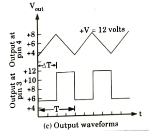
- 5. The square-wave output of Schmitt trigger, inverted and buffered is available at pin 3.
- 6. The waveforms at the output pins 3 and 4 are shown in Fig.(c).
Q5. Write a note on Ex-OR as a phase detector.
Ans.
- 1. The Exclusive-OR Ex-OR phase detector is shown in Fig. The output of gate circuit is high only when any one of the two namely input signals, fo or fi is high.
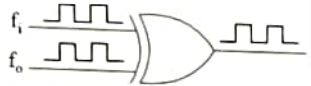
- 2. The input and output waveform for fi = fo are shown in Fig. In a digital phase detector, the phase error 𝝓 is defined as
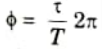
where T is the period of input signals of same frequency and 𝝉 is the time difference between the leading edges of the two signals.
- 3. Fig. shows that fo leads fi by 𝝓 degrees and the DC output of voltage the Ex-OR gate is a function of the phase error between the two inputs.
- 4. Ex-OR phase detector can be realized using ICs such as CD4070. The output DC voltage depends on the duty cycle of the input waveforms. Therefore, this type of phase detector is employed when the waveforms of fo and fi are of square waveform with 50 % duty cycle.
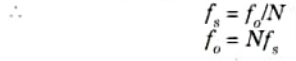
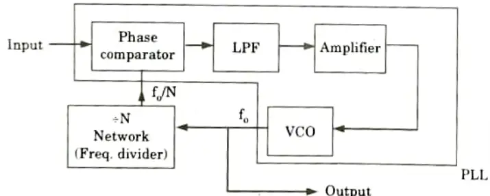
Q6. Explain the application of PLL as frequency multiplier with suitable circuit diagram.
Ans.
- 1. A divide by N network is connected externally between VCO output and phase comparator input as shown in Fig.
- 2. Since the output of the divider network is locked to input frequency fs, VCO actually operates at a frequency which is N times higher than fs.

Integrated Circuits Btech Quantum PDF, Syllabus, Important Questions
| Label | Link |
|---|---|
| Subject Syllabus | Syllabus |
| Short Questions | Short-question |
| Question paper – 2021-22 | 2021-22 |
Integrated Circuits Quantum PDF | AKTU Quantum PDF:
| Quantum Series | Links |
| Quantum -2022-23 | 2022-23 |
AKTU Important Links | Btech Syllabus
| Link Name | Links |
|---|---|
| Btech AKTU Circulars | Links |
| Btech AKTU Syllabus | Links |
| Btech AKTU Student Dashboard | Student Dashboard |
| AKTU RESULT (One VIew) | Student Result |