
“Use our AKTU question paper and solution to learn more about the exciting world of Integrated Circuits. The mysteries of electronic circuits are introduced to young brains with notes in a user-friendly PDF.
Dudes 🤔.. You want more useful details regarding this subject. Please keep in mind this as well.

Important Questions For Integrated Circuits:
*Quantum          *B.tech-Syllabus
*Circulars           *B.tech AKTU RESULT
* Btech 3rd Year
Section A: Integrated Circuits Short Questions
a. What is meant by the term matched transistors.
Ans. When two transistors are intended to be equivalent, i.e., the same size, orientation, and surroundings, as well as having identical values of saturation current, current gain, and early voltage, they are referred to as matched transistors.
b. What is a Current Mirror circuit ? Give its need.
Ans. Current mirror circuit: A current mirror copy of input current circuit is one in which the output current is compelled to equal the input current.
Need:
Current mirror circuits are commonly employed in integrated circuits as well as a variety of other applications where current must be balanced between two legs.
c. Define and give significance of Slew Rate.
Ans. Slew rate: Slew rate is defined as the maximum rate of change of output voltage with time. Its unit is V/μsec.
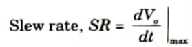
Significance: The slew rate of an ideal Op-Amp is unlimited, implying that the output voltage may instantly follow changes in the input step voltage. The higher the value of slew rate, the better the performance of the Op-Amp.
d. What do you mean by the quadrant operation of multiplier?
Ans. 1. The quadrant specifies the circuit’s suitability for bipolar signals at its inputs.
2. Only positive input signals are accepted by the first quadrant device, one bipolar signal and one unipolar signal by the second quadrant device, and two bipolar signals by the fourth quadrant device.
e. What do you mean by a frequency response of a filter circuit?
Ans. 1. Frequency response is a quantitative measure of a filter circuit’s output spectrum in response to a stimulus that is used to characterize the system’s dynamic.
2. It is a measure of the magnitude and phase of the output in relation to the input as a function of frequency.
f. Differentiate wide band and narrow band pass filter.
Ans.
| S. No. | Wide band pass filter | Narrow band pass filter |
| 1. | The wide band pass filter uses two Op-Amp. | The narrow band pass filter uses one Op-Amp. |
| 2. | It has one feedback path. | It has two feedback path. |
| 3. | The Op-Amp in the non- inverting configuration. | The Op-Amp in the inverting configuration. |
g. What role does PDN play in CMOS implementation?
Ans. The function of PDN is to provide connection between GND and Vout to pull Vout to logic. 0.
h. Differentiate between a peak detector and sample and hold circuit.
Ans.
| S. No. | Peak detector | Sample and hold circuit |
| 1. | Peak detector circuits are used to determine the peak value of an input signal | Sample and hold circuit is used to sample the given input signal and to hold the sampled value. |
i. Describe the need of voltage limiter circuits.
Ans. To limit the voltage level, a voltage limiter is utilised. When a constant, dependable voltage is required, a voltage limiter is the preferred device.
j. List the application of PLL.
Ans.
- i. Frequency multiplication/division
- ii. Frequency translation
- iii. AM detection
- iv. FM demodulation
Section B: Integrated Circuits Long Questions
a. Find out the overall gain of an op-amp IC741 giving its cascaded equivalent circuit derived for its three stages. Also drive the relationship between fT and Slew Rate for IC741.
Ans. A. Overall gain of an Op-Amp IC-741:
The overall voltage gain Av of the Op-Amp is the product of voltage gains of each stage as given by,
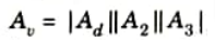
where, Ad = Gain of differential amplifier stage
A2 = Gain of the second stage
A3 = Gain of the output stage
B. Slew rate: The slew rate is defined as the maximum rate of change of output voltage per unit of time and is expressed in volts per microsecond, i.e.,

C. Relationship between ft and SR:
1. Consider a voltage follower shown in Fig.(a). The input is large amplitude, high frequency sine wave.
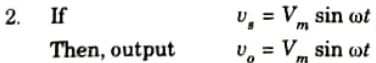
3. Fig.(b) shows the input-output waveform. Then, output
4. The rate of change of the output is given by,
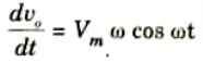
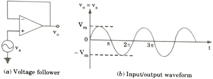
5. The maximum rate of change of the output occurs when cos ωt = 1. That
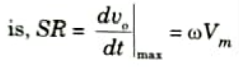
6. Therefore, slew rate
where, f = Input frequency (Hz)
Vm = Peak output amplitude.
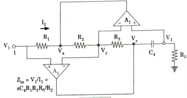
b. Draw the generalized impedance converter and derive its impedance equation. Also simulate an Inductor.
Ans. Generalized impedance converter:
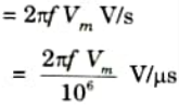
1. Generalized impedance converters (GICs) are Op-Amp circuits that employ RC networks for simulating frequency-dependent impedance elements such as inductors. Fig. shows the circuit of a GIC.
2. From Fig. at node 1,
where V1 = Vcc and V2 = V01. Now, between nodes 2 and 4, we obtain (using KCL)
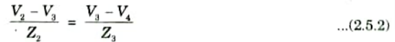
3 From the Fig. we observe that nodes 1 and 3 are virtually shorted, and hence using KCL
where V02 = V4
4. Rearranging eq.(2.5.3) yields

5. Now by using KCL between nodes 4 and 5, we have
6. Substitution for V5 = Vcc and rearrangements give
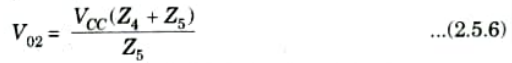
7. Substituting for V02 from eq. (2.5.6) into eq. (2.5.4), we get
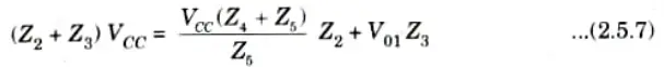
8. Rearranging eq. (2.5.7), we have
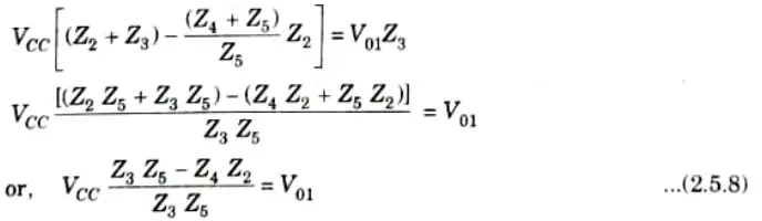
9. Substituting for V01 from eq. (2.5.8) into (2.5.1) and simplifying, we obtain
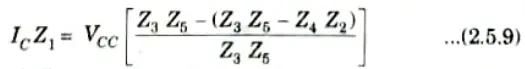
10. Rearrangement of eq. (2.5.9) yields the input impedance of the circuit
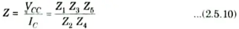
11. Eq. (2.5.10) shows that the circuit shown in Fig. can be used as grounded impedance whose nature and value depends on the nature and values of impedance elements Z1 to Z5.
Simulate an Inductor: Fig. shows the Antoniou inductance simulation circuit.
c. Describe temperature compensated Log amplifier using two op-amp and explain its operation.
Ans. 1. The logarithmic amplifier is very sensitive to temperature. To minimize the temperature effects, the circuit called temperature-compensated logarithmic amplifier is used, in which two matched diodes are used to cancel the temperature-dependent offset term ‘log Is’.
2. Similarly, a thermistor, which is a temperature-sensitive resistor can be used to cancel the temperature-dependent scaling factor ‘ηVT’
3 The output voltage of Op-Amp A1 ia negative of the voltage across diode D1 and is given by
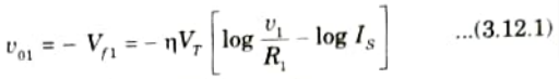
4. Similarly, the voltage across diode D2 is given by

where I is the forward current and IS is the reverse saturation current of diode D2
5. As both diodes are matched, their reverse saturation currents are same. The voltage at the non-inverting terminal of Op-Amp A2 is given by
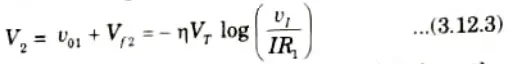
6. Thus, the temperature-dependent offset term is eliminated from the output of A1. The Op-Amp A2 isa non-inverting amplifier and its output is given by
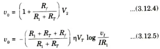
7. Thus the circuit shown in Fig. cancels the temperature-dependent terms present at the output of the log amplifier and provides a temperature-independent logarithmic output.
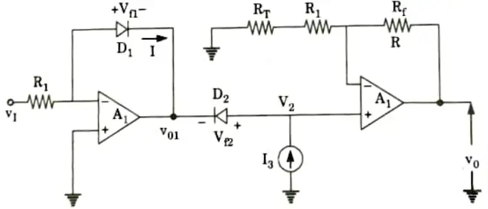
d. Sketch the logic gate symbolic representation of clocked SR flip-flop using NAND gate. Also sketch its CMOS circuit implementation and explain its operation.
Ans. A. Clocked SR flip-flop using NAND gate: Fig. shows gate level schematic of clocked NAND based SR flip-flop circuit.
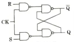
B. CMOS Implementation:
1 A simpler implementation of a clocked SR flip-flop is shown in Fig. Here, pass transistor logic is employed to implement the clocked set-reset function.
2. The SR flip-flop comprising two cross-coupled inverters and two pass transistors Q5 and Q6 The pass transistors are turned ON when the clock (ɸ) is high, and they connect the flip-flop input S and R. The pass transistors act as transmission gates allowing the inputs S and R.
C. Operation:
- 1. Consider the flip-flop output has the initial state Q = 1 and Q(bar) = 0, and the input R = 1 and S = 0 is applied to the input of flip-flop.
- 2 When the clock ɸ is high, the transIstors Q5 and Q6 are turned ON
- 3. For this input R= 1 and S =0, the transistor Q3 is turned ON and pull down the out put Q = 0.
- 4. These output Q is applied to the input of Q2 and Q1 transistors, this will make the transistor Q2 is turned ON and the output Q(bar) becomes high.
- 5. Now consider the output has initial state Q = 0 and Q(bar) = 1, and the input R= 0 and S = 1. When the clock ɸ is high, the pass transistors Q5 andQ6 are turned ON. For this input R = 0 and S =1, the transistor Q1 turned ON and Q2 is turned OFF.
- 6. This causes the output Q(bar) = 0 and Q(bar) is applied to the input of transistors Q3 and Q4. Now the transistor Q4 turned ON and this make the output Q is high.
e. Draw the block diagram of a PLL and explain its operation. Explain lock-in-range, capture range and pull-in time of a PLL.
Ans. A. Principle of operation of PLL:
- 1. The two inputs of the phase detector or comparator are the input voltage Vs at frequency fs and the feedback voltage from a voltage controlled oscillator (vcO) at frequency fo.
- 2. The phase detector compares these two signals and produces a DC voltage Ve which is proportional to the phase difference between fs and fo.
- 3. The output voltage Ve of the phase detector is called as error voltage. This error voltage is then applied to low-pass filter.
- 4. Low-pass filter removes the high frequency noise present in the phase detector output and produces a ripple free DC level.
- 5. This DC level is amplified to an adequate level by the amplifier and applied toa VCO.
- 6. The DC amplifier output voltage is called as the control voltage VC.

- 7. The control voltage VC is applied at the input of a VCO. The output frequency of VCO is directly proportional to the DC control voltage VC.
- 8. The VCO frequency fo is compared with the input frequency fs by the phase detector and it is adjusted continuously until it is equal to the input frequency fs i.e.. fo = fs
- 9. Once, the action of shifting VCO frequency in a direction to reduce the frequency difference between fs and fo starts, we say the signal is in the capture range.
- 10. When the output frequency is exactly the same as the input frequency, PLL is then said to be locked.
- 11. Once locked the output frequency fo is identical to fs except for a finite phase difference.
- 12. This phase difference generates a control voltage VC to shift VCOD frequency from fo to fs thereby maintaining the lock. Once locked, PLL tracks the frequency changes of the input signal.
B. Lock-in range: Once locked, the PLL can track frequency variations in incoming signals. The frequency range across which the PLL can keep lock with the incoming signal is referred to as the lock-in range or tracking range.
C. Capture range: The range of frequencies over which the PLL can acquire lock with an input signal is called the capture range.
D. Pull-in time: The overall time required by the PLL to establish lock is referred to as pull-in time. The initial phase and frequency difference between the two signals, as well as the loop gain and loop filter parameters, all influence this.
E. Applications:
- 1. Frequency divider
- 2. Frequency multiplier
- 3. Frequency synthesizer
- 4. AM detector
- 5. FM detector
- 6. FSK demodulator.
Section 3: BJT Complementary Push-Pull Output Stage
a. Describe the operation and characteristics of a BJT complementary push-pull output stage.
Ans. Fig.1 shows a class B output stage. It consists of a complementary pair of transistors (npn and pnp) connected in such a way that both cannot conduct simultaneously.
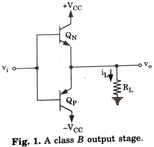
Operation:
- 1. When the input voltage vi is zero, both transistors are cut-off and the output voltage vo is zero.
- 2. As vi goes positive and exceeds about 0.5 V, Q, conducts and operates as an emitter follower. In this case vo follows vi (i.e., vi = vo – vBEN) and QN supplies the load current.
- 3. Meanwhile, the emitter-base junction of QP will be reverse-biased by the VBE of QN, which is approximately 0.7 V. Thus QP will be cut-off.
- 4. If the input goes negative by more than about 0.5 V, QP turns ON and acts as an emitter follower.
- 5. Again vo follows vi (.e., vo = vi + vEBP), but in this case Qp supplies the load current and QN will be cut-off.
- 6. We conclude that the transistors in the class B stage of Fig. 2 are biased at zero current and conduct only when the input signal is present.
- 7. The circuit operates in a push-pull fashion:
- i. QN pushes (sources) current into the load when vi is positive, and
- ii. QP pulls (sinks) current from the load when vi is negative.
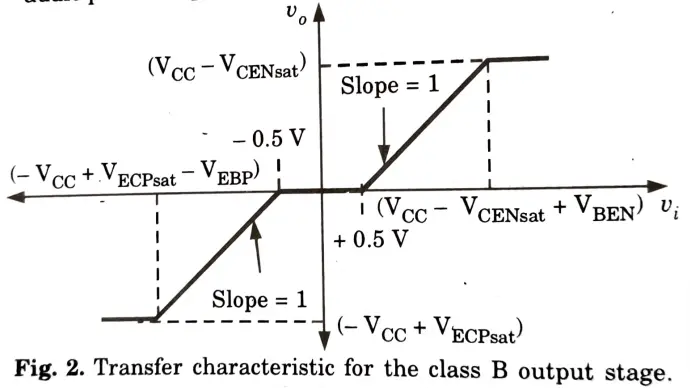
Transfer characteristic:
- 1. In Fig. 2 there exists a range of vi centered around zero where both transistors are cut-off and vo is zero. This dead band results in the cross-over distortion.
- 2. The effect of cross-over distortion will be most pronounced when the amplitude of the input signal is small. Cross-over distortion in audio power amplifiers gives rise to unpleasant sounds.
b. Give circuit description of IC741 with the help of its block diagram.
Ans. A. Op-Amp circuit:
- 1. Generally BJT based Op-Amp is focused on 741 Op-Amp circuit. If we use IC design, the circuits use large number of transistors but relatively few resistors and only one capacitor.
- 2. The block diagram of typical Op-Amp is shown in Fig.
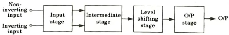
- 3. The equivalent circuit of Op-Amp is shown in Fig.
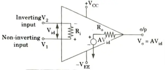
B. Characteristics of ideal Op-Amp:
- 1. Infinite voltage gain, Av = ∞.
- 2. Infinite input resistance, Ri = ∞.
- 3. Zero output resistance, Ro = 0.
- 4. Zero output voltage when input voltage is zero.
- 5. Infinite bandwidth.
C. Bias circuit:
- 1. A bias circuit is utilized to provide proportionate current in a transistor’s collector.
- 2. Certain transistors form a current mirror, in which the transistor collector generates bias current for the Op-other Amp’s output stage.
- 3. Finally some transistors works to provide the VBE drop between the bases of output transistors for proper functioning of the device.
Section 4: Narrow Band Reject Filter
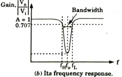
a. Draw and explain Narrow Band Reject Filter. Also, find its transfer function.
Ans. A. Band-reject filter:
The band-reject filter, also known as the band-elimination or band-stop filter, attenuates frequencies in the stopband and allows them to pass outside of it.
B. Types:
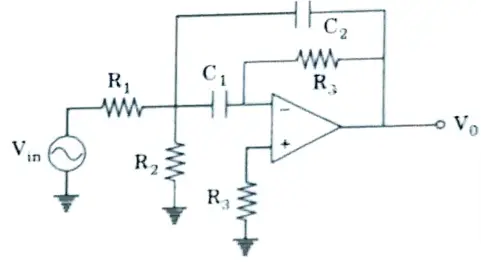
i. Narrow band-reject filter:
1. The narrow band-reject filter, often called the notch filter, is the twin T network cascaded with the voltage follower as shown in Fig.(a).
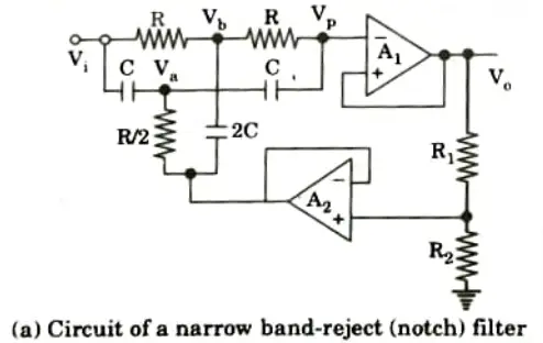
2. Applying Kirchhoff’s current law at node Va, we get

3. Applying Kirchhoff current law at node Vb we get
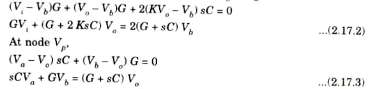
4. From the above three node voltage eq. (2.17.1), (2.17.2) and (2.17.3), the transfer function can be written as
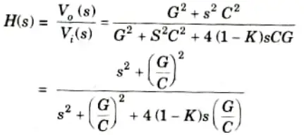
5. In the steady-state, that is s = jω,
6. At 3 dB cut-off frequency,
8. Upon solving the above quadratic equation, we obtain the upper and lower half power frequencies as,
9. The 3 dB bandwidth is
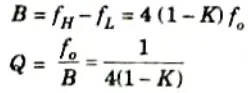
ii. Wide band-reject filter:
1. Fig.(a) shows a wide band-reject filter that is obtained by paralleling a high-pass filter with a cut-off frequency of f with a low-pass filter.
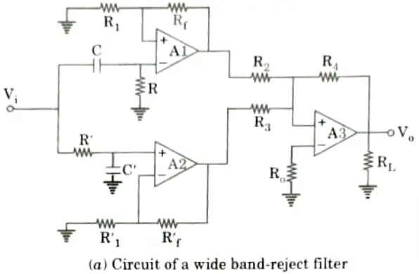
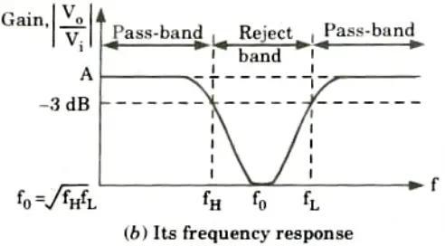
2. With cut-off frequency of fH provided fL > fH and a summing amplifier connected in series to add the filtered individual passband components.
3. The passband gains of both the high-pass and low-pass sections must be equal.
4. The frequency response characteristic of the wide band-reject filter is shown in Fig.(b).
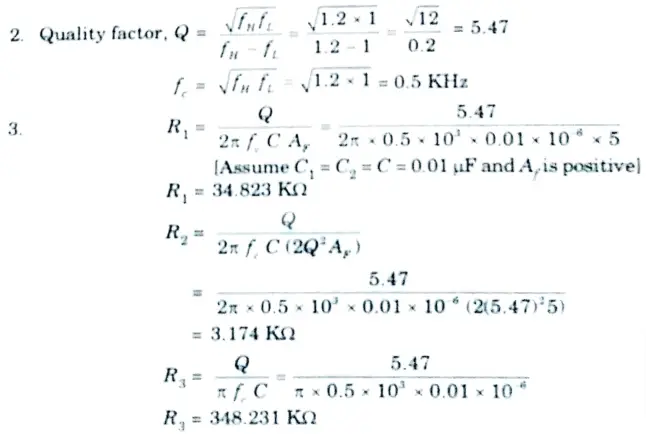
b. Compare and contrast active filters and passive filters. Design band pass filter with single op-amp for the given specifications : fL – 1 KHz; fH = 1.2 KHz, AF =- 5.
Ans. A. Comparison:
| S. No. | Active filter | Passive filter |
| 1. | Active filters have a power gain i.e., can add energy into the circuit. | Passive filters cannot cause power gain, i.e., they cannot bring energy into the circuit. |
| 2. | Active filters require an external power supply. | Passive filters do not require any external power. |
| 3. | Active filters have frequency limitation due to active elements. | Passive filters have no frequency limitations. |
| 4. | It provides complex control system and therefore expensive than passive filters. | Passive filters are relatively heaper than active filters. |
B. Numerical:
1. The narrow band pass filter is shown in Fig.
Section 5: GILBERT Analog Multiplier
a. Draw the circuit diagram for monostable multivibrator with operational amplifier. Explain its operation. Derive the expression for its time period.
Ans. A. Monostable multivibrator:
- 1. Fig. shows the circuit diode diagram of monostable multivibrator. A D1 clamps the capacitor voltage to 0.7 V when the output is at +Vsat.
- 2. The negative going pulse signal of magnitude V1 (triggering signal) passing through the differentiator R3C1 and diode D2 produces a negative going triggering pulse and is applied to the (+) input terminal.
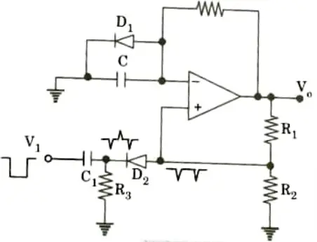
B. Operation:
- 1. For monostable operation, the trigger pulse width Tp should be much less than T, the pulse width of the monostable multivibrator.
- 2. The diode D2 is used to avoid malfunctioning by blocking the positive spikes that may be present at the differentiated trigger input.
- 3. Fig. shows the trigger and output waveform.
- 4. When Vo is +Vsat, voltage divider R1 and R2 feedback VUT to the (+ve) input. The diode D1 clamps the (-ve) input at approximately 0.7 V (because the diode is forward biased).
- 5. The feedback voltage at (+ve) terminal is higher than (-ve) terminal therefore Op-Amp holds Vo at +Vsat This output state is called as stable state.
- 6. If the negative spike (trigger signal) is applied to (+ ve) of Op-Amp which is higher than the voltage at (-ve) terminal. The combination o feedback voltage and negative trigger voltage will be pulled below the voltage at (-ve) input.
- 7. Once the (+ ve) input becomes negative with respect to the (- ve) input, Vo switches to -Vsat With this change, the one-shot is now in its timing state. This state is an unstable state.
- 8. Due to Vo = – Vsat, the diode D1 is reverse biased and the capacitor C charges, the -ve) input. The (- ve) input becomes more and more negative with respect to ground. When the capacitor voltage is more than (+ ve) terminal, Vo switches to + Vsat.
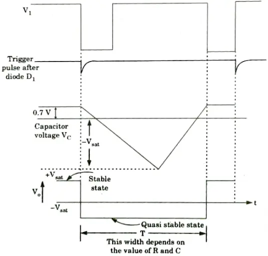
C. Expression for time period :
1. The general solution for a signal time constant low pass RC circuit with Vi and Vf as initial and final value is

The output VC is

If the time constant T = RC and when t = T
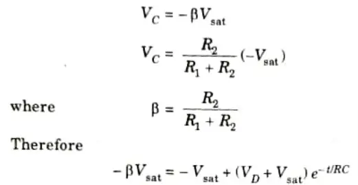
4. After simplification, the pulse widths is obtained as
b. What do you mean by the quadrant operation of multiplier? Draw and explain a GILBERT analog multiplier.
Ans. A. Quadrant operation of multiplier:
- 1. The quadrant specifies the circuit’s suitability for bipolar signals at its inputs.
- 2. Only positive input signals are accepted by the first quadrant device, one bipolar signal and one unipolar signal by the second quadrant device, and two bipolar signals by the fourth quadrant device.
B. GILBERT analog multiplier:
- 1. The GILBERT multiplier cell is an emitter coupled cell modification that allows for four-quadrant multiplication. As a result, it serves as the foundation for the majority of integrated circuit balanced multipliers.
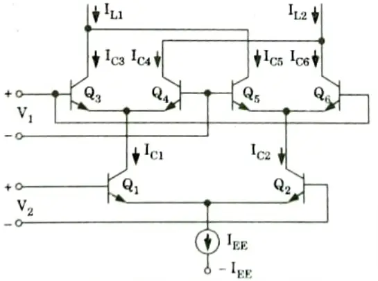
- 2. The GILBERT multiplier cell is made up of two cross-coupled emitter-coupled pairs connected in series with an emitter coupled pair.
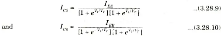
- 3. The collector currents of Q3 and Q4 are given by
- 4. Similarly the collector currents of Q5 and Q6 are given by
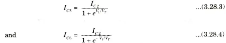
- 5. The collector currents IC1 and IC2 of transistors Q1 and Q2 can be expressed as
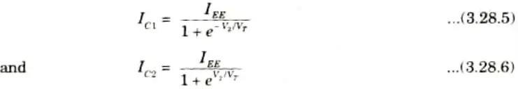
- 6. Substituting eq. (3.28.5) in eq. (3.28.1) and (3.28.2), we get
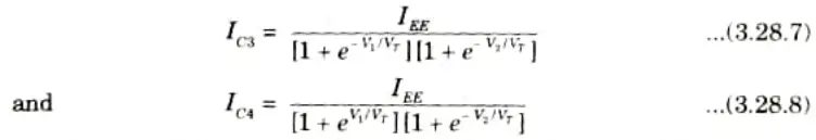
- 7. Similarly, substituting eq. (3.28.6) in eq. (3.28.3) and (3.28.4), we get
- 8. The differential output current 𝚫l is given by
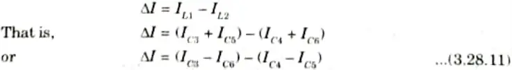
- 9. Substituting eq. (3.28.7) to (3.28.10) in eq. (3.28.11) and employing exponential formulae tor hyperbolic functions, we get
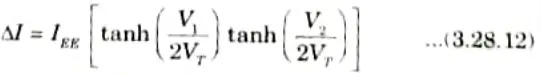
eq. (3.28.12) shows that when V1 and V2 are small, the GILBERT cell shown in Fig. can be used as a four-quadrant analog multiplier with the use of current-to-voltage converters.
Section 6: Features of CMOS Circuit
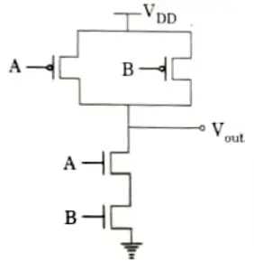
a. Explain the structure and operation of CMOS inverter. Realize the circuit of 2 input NOR gate and 2 input NAND gate using CMOS and explain the operation.
Ans. A. CMOS inverter:
CMOS inverter circuit:
- 1. Fig. shows the CMOS inverter. In the CMOS inverter, the PMOS and NMOS devices QP and QN are driven simultaneously by an input
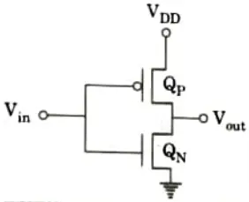
Working operation:
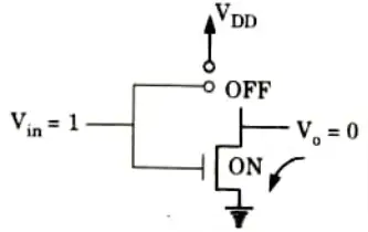
1. When input is high (≃ VDD)QN is made to conduct, while QP is forced to cut-off. This causes the output becomes low (Vo = 0) as shown in Fig.
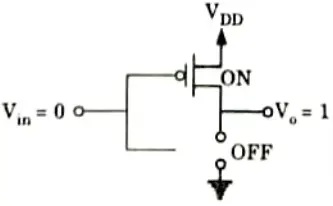
2. When input is low (≃ VDD)QN is OFF and QP becomes ON, therefore the output becomes logic high (Vo = VDD) as shown in Fig.
3. Table shows the operation of CMOS inverter circuit.
| Vin | QP | QN | Vo |
| 0 | ON | OFF | 1 |
| 1 | OFF | ON | 0 |
B. Realize of 2 input NOR gate and 2 input NAND gate:
2 input NOR gate:
Realization of 2 input NOR gate circuit is shown in Fig.
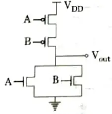
Operation: The logic operation of NOR gate is such that the output is HIGH only when all inputs are LOW for remaining all other conditions, the output is LOW.
2 input NAND gate:
Realization of 2 input NAND gate circuit is shown in Fig.
Operation: A NAND gate produces a LOW output only when all the inputs are HIGH. When any of the inputs is LOW, the output will be HIGH.
b. Discuss the features of CMOS circuit. Describe D-F/F circuit using NAND CMOS gates.
Ans. A. Features of CMOS circuit:
- 1. The output is always connected to VDD or GND and in steady state; it gives full logic swing (between 0 V and VDD) voltage transfer characteristics and large noise margins.
- 2. Logic levels are not dependent upon the relative sizes of the devices.
- 3. There is no direct path between VDD and GND in steady state. Thus, static power dissipation of CMOS circuit is negligible.
- 4. It has high input impedance and fast switching speed.
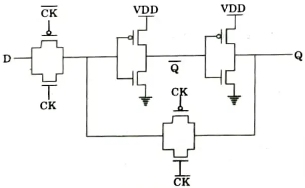
B. D-FF circuit using NAND CMOS gates:
- 1. Fig. shows the circuit realization of D flip-flop with CMOS NAND gate. This circuit consists of two stages implemented by SR NAND latches.
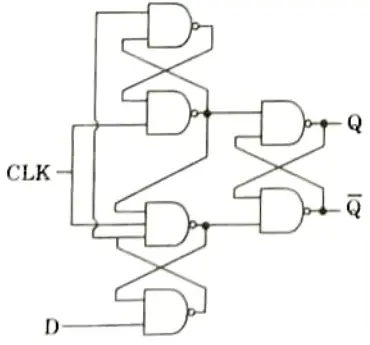
- 2. The input stage (the two latches on the left) processes the clock and data inputs to guarantee that the output stage receives the correct input signals (the single latch on the right).
- 3. If the clock is low, independent of the data input, both output signals of the input stage are high; the output latch is unaffected and stores the prior state.
- 4. When the clock signal changes from low to high, only one of the output voltages (depending on the data signal) goes low and set/resets the output latch. If D =0, the lower output becomes low; if D= 1, the upper output becomes low.
- 5. If the clock signal is high, the outputs retain their states regardless of the data input, and the output latch is forced to remain in the matching state since the input logical zero remains active while the clock is high.
- 6. Hence the role of the output latch is to store the data only while the clock is low.
- 7. The D latch is normally, implemented with transmission gate (TG switches as shown in the Fig.
Section 7: Block Diagram of IC 555
a. Explain the block diagram of IC 555. Design a 555 timer as astable multivibrator with an output signal with frequency 2 KHz and 75 % duty cycle.
Ans. A. Block diagram of IC 555:
- 1. In the stable state, the output Q(bar) of the flip-flop (FF) is high. This makes the output low because of power amplifier which is basically an inverter.
- 2. If negative going trigger pulse is applied to pin 2 and should have its DC level greater than the threshold level of the lower comparator (i.e.. VCC/3), now the trigger passes through (Vcc/3), the output of the lower comparator goes high and sets the FF (Q = 1,Q(bar) = 0). Therefore the output of IC 555 becomes high.
- 3. When the threshold voltage at pin 6 passes through (23) VCC the output of the upper comparator goes high and resets the PF (Q = 0,Q(bar) = 1).
- 4. The reset input (pin 4) is used to reset the FP and the flip fop output Q(bar) becomes high and the output of IC 666 becomes low because the output of FF is 1.

B. Numerical:
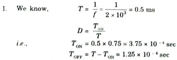
2. Duty cycle is more than 50 % hence modified circuit must be used.
3 The modified circuit is shown in Fig.
4. Let C = 0.01 𝛍F
The charging of C takes place through R1 and diode D while discharging takes place through R2 only
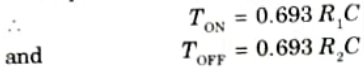
5. Using values of TON, TOFF and C,
R1 = 8.658 k𝛺
and R2 = 20.202 k𝛺
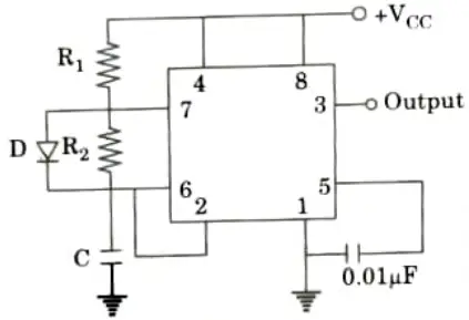
b. Describe the working of an VCO with the help of functional block diagram of VCO IC 566.
Ans.
- 1. The pin configuration and the basic block diagram of IC 566 VCO are shown in the Fig. (a) and (b) respectively. The frequency of oscillation is determined by an externally connected resistor R1 and a capacitor C1.
- 2. The control voltage or the modulating input vc is applied at the control terminal (pin 5).
- 3. The triangular voltage obtained at pin 4 is shown in Fig. (c). It is generated by alternately charging the capacitor C1 by one current source, and discharging it linearly through another current source. The amount of charge and discharge voltage swing is determined by the Schmitt trigger.
- 4. The Schmitt trigger also provides the square-wave output at pin 3 through the power amplifier A3 and the triangular output is available at pin 4 through the buffer amplifier A1.
Operation of VCO:
- 1. The output voltage swing of the Schmitt trigger is set to the levels Vcc and 0.5 Vcc. In Fig. if Ra = Rb in the positive feedback path, the voltage at the non-inverting terminal of Op-Amp A2 swings from 0.5 Vcc to 0.25 Vcc.
- 2. During charging of C1 when the voltage across C1 just exceeds 0.5 Vcc the Schmitt trigger switches to LOW (0.5 Vcc) and the capacitor starts discharging.
- 3. When the voltage across C1 reduces to 0.25 Vcc the Schmitt trigger switches to HIGH (Vcc).
- 4. By maintaining the source current and sink current of the two current sources equal, a uniform triangular voltage with equal positive and negative slopes is obtained at pin 4.
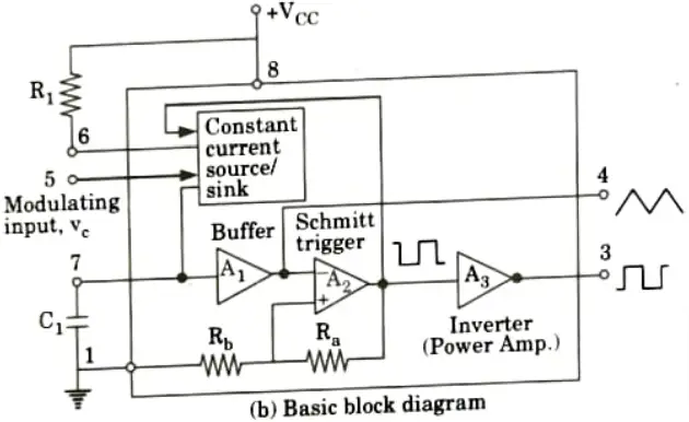
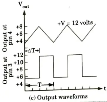
- 5. The square-wave output of Schmitt trigger, inverted and buffered is available at pin 3.
- 6. The waveforms at the output pins 3 and 4 are shown in Fig. (c).
6 thoughts on “Integrated Circuits: Aktu Previous Solved Question Paper, Notes”