Aktu Btech Quantum Notes will take you on a journey through VLSI technology. Using these important, often asked questions, you may master key topics and excel in tests. Begin your path to success right now! Unit-1 Introduction to IC Technology
Dudes 🤔.. You want more useful details regarding this subject. Please keep in mind this as well.

Important Questions For VLSI Technology:
*Quantum             *B.tech-Syllabus
*Circulars              *B.tech AKTU RESULT
* Btech 3rd Year   * Aktu Solved Question Paper
Q1. Define the term: SSI, MSI, LSI, VLSI and ULSI.
Ans. Depending upon the number of active devices per chip, there are different levels of integration :
- i. SSI: Small scale integration occurs when there are less than 100 active devices per chip (SSD). Integral resistors, diodes, and bipolar transistors are used in the majority of SSI devices.
- ii. MSI: Medium scale integration occurs when there are between 100 and 1000 active devices per chip (MS). BJTs and enhancement mode MOSFETs are integrated in the majority of MSI chips.
- iii. LSI: The range of active devices per chip in large scale integration (LSI) is between 1000 and 100,000. MOS transistors are typically used in LSI devices because they require fewer integration stages. As a result, MOS transistors are able to create more components per chip than bipolar transistors.
- iv. VLSI: Very high scale integration occurs when there are over hundreds of thousands of active devices on each chip (VLSI). Modern chips almost universally use the VISI method.
- v. ULS: Recently a new level of integration has been introduced which is known as ultra large scale integration (ULSD. In ULSI technique, more than one million active devices are integrated on a single chip. Pentium microprocessors use ULSI technology.
| S. No. | Level of integration devices per chip | Number of active |
| 1. | Small scale integration (SSI) | less than 100 |
| 2. | Medium scale integration (MSI) | 100 – 10000 |
| 3. | Large scale integration (LSI) | 1000 – 100000 |
| 4. | Very large scale integration (VLSI) | Over 100000 |
| 5. | Ultra large scale integration (ULSI) | Over 1 million |
Q2. Write a short note on Czochralski process.
Ans.
- 1. Fig. shows the schematic of a CZ system which can be used for beth silicon and GaAs crystal growth. Here, the melt is contained in a crucible and kept in molten condition by heating.
- 2. A seed crystal. suitably oriented, is suspended over the crucible in a chock. For growth, the seed is inserted into the melt until its end is molten.
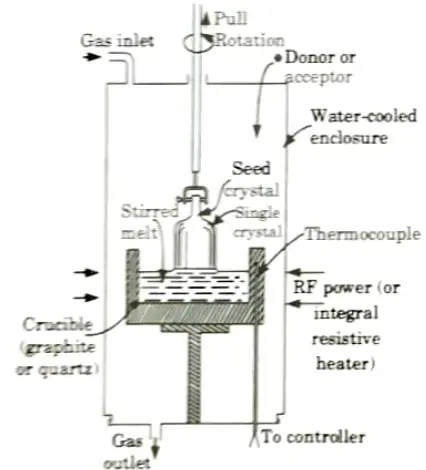
- 3. It is now being discontinued gradually. resulting in the formation of a single crystal that develops through gradual freezing at the liquid-solid interface. For both silicon and gaAs, a pull rate of roughly 50-100 mm/hr is normal.
- 4. During the pulling process, it is also possible to rotate the crystal and occasionally the crucible.
- 5. To manage radial temperature gradients during the solidification process, a series of annular heat shields are installed between the growing region and the reactor walls.
- 6. For silicon, the complete system is encased in a water-cooled and inert gas flushed enclosure.
- 7. With GaAs, on the other hand, it’s crucial to maintain an arsenic overpressure of roughly 1.0 atm in order to prevent melt breakdown during crystal formation.
- 8. During the development process, the latent heat of fusion must be eliminated from the crystal-melt system. Thermal conduction along the crystal axis and radiation from the crystal’s surface both contribute to the loss of this heat.
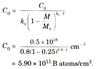
Q3. A silicon ingot with 0.5 x 10¹⁶ boron atoms/cm3 is to be grown by CZ method. What should be the concentration of boron in the melt to obtain the required doping concentration? The segregation coefficient of the boron is 0.8.
Ans. Given: CS = 0.5 x 10¹⁶ B atoms/cm3, kc = 0.8 for boron
To Find: Concentration of boron.
1. The concentration of dopant in the solid phase of silicon is given by
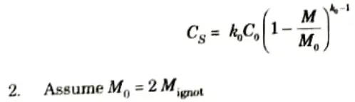
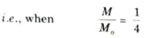
3. We want a concentration of CS = 0.5 x 10¹⁶ atoms of B/cm3 halfway through the final grown ingot,
4. The initial concentration of B atoms in the melt should be,
Q4. Discuss the crystal hardening techniques.
Ans.
- 1. The generation of thermally induced glide dislocations can be reduced if the crystal is strengthened, so as to increase its critical resolved shear stress.
- 2. In silicon growth, for example, this occurs to some extent by the incorporation of oxygen due to the corrosive action of the SiO2 crucible walls.
- 3. In GaAs, the intentional doping with group III and V impurities has been used for this purpose.
- 4. At the moment, the mechanism of solution hardening is not fully understood.
- 5. It has been suggested that it results from the strain field produced by the lattice mismatch caused by the impurity, which prevents dislocations from spreading after they have been formed.
- 6. This technique’s success may be explained by the fact that dislocations’ energy of movement is significantly lower than their energy of production.
- 7. There are several reasons why isoelectronic doping is not employed commercially.
- 8. Although being practically dislocation-free, the material is very brittle, making it difficult to fabricate into slices and prone to fracture during the manufacturing of devices.
- 9. The lattice parameter of the GaAs is then increased by the addition of indium, resulting in lattice mismatch conditions for any further growth on the surface.
- 10. In the end, it was demonstrated that GaAs crystals produced by twofold annealing could satisfy the criteria for field effect transistor threshold voltage uniformity throughout a slice without the necessity for solid solution hardening.
Q5. Discuss the processing considerations of silicon wafers.
Ans. In the IC processing of silicon wafers, it is usually necessary to maintain the purity and perfection of the material and it is done by three methods:
i. Chemical cleaning:
- 1. Organic coatings, heavy metals, and particles are often removed from silicon wafers via chemical cleaning.
- 2. Organic pollutants will also be eliminated by mixes based on ammonium hydroxide and sulfuric acid.
- 3. Since peroxide is an oxidizer, these cleaning agents leave the surface of a wafer in a hydrophilic state.
- 4. The chemically generated oxide is often removed by a brief immersion in diluted hydrofluoric acid because it may include chemical contaminants.
ii. Gettering Treatments:
- 1. A large number of VLSI circuits demand low junction leakage currents. Conductive impurity precipitates, which function as shorts between the emitter and collector, can affect narrow base bipolar transistors and cause them to malfunction.
- 2. These components serve as hubs for carrier production and recombination and are found at interstitial or substitution lattice sites.
- 3. The term “gettering” is used to describe a technique that clears dangerous contaminants or flaws from the wafer regions where devices are manufactured.
- 4. Pretreatment methods for silicon wafers before IC processing are among these methods. A wafer with pregettering has sinks that can take in impurities when they are added during device production.
- 5. One method of purging contaminants includes purposefully scratching the wafer’s rear surface. For this, mechanical abrasion techniques like lapping and sandblasting have been employed.
- 6. Damage produced by a focussed heat beam is used in a more regulated method. The necessary energy density for this operation is 5 J/cm2.
- 7. One implementation of this method uses a Q-pulsed Nd:YAG laser. The array of micromachined dots is produced by rastering the laser beam across the rear surface.
- 8. Depending on the energy density and closeness of the spots, the high-energy pulse can damage or strain the silicon lattice.
- 9. The spots produce dislocations as they undergo thermal processing. The dislocations stay isolated on the back surface if the forces applied to the wafer during furnace processing are minimal.
- 10. The dislocations serve as good trapping grounds for quickly dispersing animal. These contaminants are harmless when they are trapped on the back surface.
iii. Thermal stress:
- 1. In furnaces, wafers are usually treated on racks with a large wafer diameter to spacing ratio.
- 2. The wafer centres stay relatively hot after being taken from a high temperature furnace, while the wafer edges rapidly cool by radiation to the surroundings.
- 3. The resultant temperature gradient creates a thermal stress S that can be estimated as
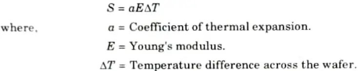
- 4. By slowly removing wafers from the furnace to reduce temperature gradients or by lowering the furnace temperature until the yield strength at the removal temperature surpasses the stresses imposed, stresses are typically reduced to an acceptable level.
- 5. Oxygen precipitates can reduce the yield strength up to five fold.
Q6. What is the objective of wafer cleaning ? Explain any one method of wafer cleaning.
Ans. A. Objective of wafer cleaning: The objective of wafer cleaning is the removal of particle and chemical impurities from the semiconductor surface without damaging or deleteriously altering the substrate surface.
B. RCA:
- 1. One highly successful approach to cleaning silicon, known as “RCA clean”, is to use two solutions in sequence.
- 2. The first of these consists of 1 : 1 : 5 to 1 : 2 : 7 volumes of NH4OH : H2O2:H20.
- 3. Here, the H2O2 functions to oxidize all remaining organic contaminants on the surface, which are present because of incomplete removal of photoresist, and also because of airborne materials and physical handling.
- 4. The NH4OH is effective in removing heavy metals such as cadmium, cobalt, copper, iron, mercury, nickel, and silver by forming amino complexes with them.
- 5. Next, a solution consisting of HCl : H2O2 : H2O in a 1 : 1 : 6 to 1 : 2 : 8 volume ratio is used to remove aluminum, magnesium, and the light alkali ions, and to prevent displacement replating from the solution.
- 6. Each of these steps is carried out for 10-20 min at 75-85°C, under conditions of rapid agitation. Nitrogen gas bubbling through the etchants is often used for this purpose.
- 7. Finally, wafers are blown dry and stored in a clean environment until further processing
- 8. Results with this cleaning technique make it quite suitable for bipolar as well as MOS microcircuits, so that it is in wide use in industry at the present time.

VLSI Technology Btech Quantum PDF, Syllabus, Important Questions
| Label | Link |
|---|---|
| Subject Syllabus | Syllabus |
| Short Questions | Short-question |
| Question paper – 2021-22 | 2021-22 |
VLSI Technology Quantum PDF | AKTU Quantum PDF:
| Quantum Series | Links |
| Quantum -2022-23 | 2022-23 |
AKTU Important Links | Btech Syllabus
| Link Name | Links |
|---|---|
| Btech AKTU Circulars | Links |
| Btech AKTU Syllabus | Links |
| Btech AKTU Student Dashboard | Student Dashboard |
| AKTU RESULT (One VIew) | Student Result |