
With Aktu Btech Quantum Notes, you may explore the world of Integrated Circuits. Master important concepts and ace tests with these frequently asked questions. Take advantage of them right now to ensure your success! Unit-4 Digital Integrated Circuit Design
Dudes 🤔.. You want more useful details regarding this subject. Please keep in mind this as well.

Important Questions For Integrated Circuits:
*Quantum               *B.tech-Syllabus
*Circulars                *B.tech AKTU RESULT
* Btech 3rd Year    * Aktu Solved Question Paper
Q1. Discuss CMOS circuit and its features.
Ans. A. CMOS circuit:
- 1. The CMOS logic gate consists of two networks.
- i. The pull-down network (PDN) constructed of NMOS transistor.
- ii. The pull-up network (PUN) constructed of PMOS transistors.
- 2. The two networks are operated by the input variables, in a complementary fashion.
- 3. Thus, for the three-input gate represented in Fig. the PDN will conduct for all input combinations that require a low output (Y= 0) and will then pull the output node down to ground, causing a zero voltage to appear at the output, vy = 0.
- 4. Simultaneously, the PUN will be OFF, and no direct DC path will exist between VDD and ground. On the other hand, all input combinations that call for a high output (Y = 1) will cause the PUN to conduct, and the PUN will then pull the output node up to VDD, establishing an output voltage vy = VDD.
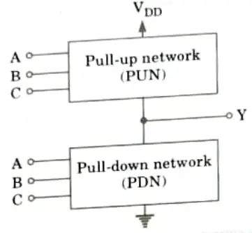
- 5. Simultaneously, the PDN will be cut-off, and again, no DC current path between VDD and ground will exist in the circuit.
B. Features:
- 1. The output is always connected to VDD or GND and in steady state; it gives full logic swing (between 0 V and VDD) voltage transfer characteristics and large noise margins.
- 2. Logic levels are not dependent upon the relative sizes of the devices.
- 3. There is no direct path between VDD and GND in steady state. Thus, static power dissipation of CMOS circuit is negligible.
- 4. It has high input impedance and fast switching speed.
Q2. Explain the effect of fan-in and fan-out on propagation delay in CMOS digital logic circuit.
Ans.
- 1. A gate’s fan-in is the total sum of all of its inputs. A CMOS gate needs two more transistors, one NMOS and one PMOS, for every additional input.
- 2. The extra transistor expands the chip’s surface area and increases the total effective capacitance per gate as well as the propagation delay.
- 3. We maintain the current-driving capabilities by enlarging the gadget.
- 4. Yet, both the increased number of inputs and the larger device size result in an increase in capacitance C. Following a quadratic function of fan-in, latency often grows.
- 5. A gate’s fan-out grows with its load, which raises its capacitance and lengthens the propagation delay.
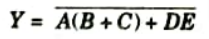
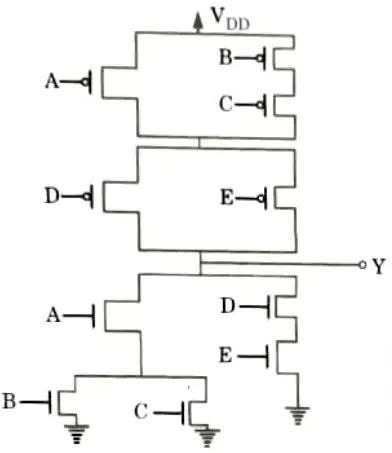
Q3. Sketch the CMOS logic circuit realization of the expression
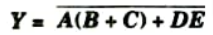
Ans. CMOS logic circuit realization of
Q4. Realize the circuit of 2 input NOR gate and 2 input NAND gate using CMOS and explain the operation.
Ans. A. 2 input NOR gate:
Realization of 2 input NOR gate circuit is shown in Fig.
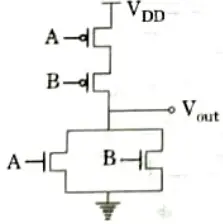
Operation: The logic operation of NOR gate is such that the output is HIGH only when all inputs are LOW for remaining all other conditions, the output is LOW.
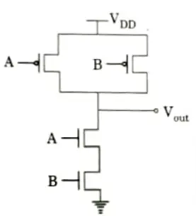
B. 2 input NAND gate:
Realization of 2 input NAND gate circuit is shown in Fig.
Operation: A NAND gate produces a LOW output only when all the inputs are HIGH. When any of the inputs is LOW, the output will be HIGH.
Q5. Discuss D-F/F circuit using NAND CMOS gates.
Ans. 1. Fig. shows the circuit realization of D flip-flop with CMOS NAND gate. This circuit consists of two stages implemented by SR NAND latches.
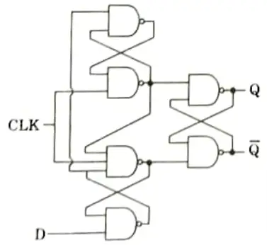
- 2. The input stage (the two latches on the left) processes the clock and data Signals to ensure correct input signals for the output stage (the single latch on the right).
- 3. If the clock is low, both the output signals of the input stage are high regardless of the data input; the output latch is unaffected and it stores the previous state.
- 4. When the clock signal changes from low to high, only one of the output voltages (depending on the data signal) goes low and set/resets the output latch. If D =0, the lower output becomes low; if D= 1, the upper output becomes low.
- 5. If the clock signal continues staying high, the outputs keep their states regardless of the data input and force the output latch to stay in the corresponding state as the input logical zero remains active while the clock is high.
- 6. Hence the role of the output latch is to store the data only while the clock is low.
- 7. The D latch is normally, implemented with transmission gate (TG) switches as shown in the Fig.
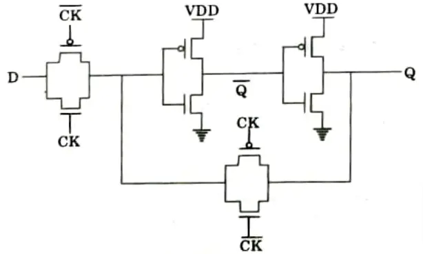
- 8. Input D is accepted when CK is high. When CK goes low, the input is open-circuited and the latch is set with the prior data D.
Q6. Give two different CMOS realization of the Exclusive-OR gate function in which the PDN and PUN are dual network.
Ans. 1. For Exclusive OR function we have,
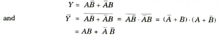
Realization I:
2. Note that Fig.(b) is drawn by converting parallel networks of Fig.(a) to serial networks.
3. Now by connecting PUN of Fig.(a) with PDN of Fig.(a) we can realize Exclusive-OR function.
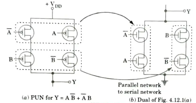
Realization II:

4. Note that Fig.(b) is drawn by converting series networks into parallel networks.
5. Now by connecting PUN of Fig.(b) with PDN of Fig.(a) we can realize Exclusive-OR function.

Integrated Circuits Btech Quantum PDF, Syllabus, Important Questions
| Label | Link |
|---|---|
| Subject Syllabus | Syllabus |
| Short Questions | Short-question |
| Question paper – 2021-22 | 2021-22 |
Integrated Circuits Quantum PDF | AKTU Quantum PDF:
| Quantum Series | Links |
| Quantum -2022-23 | 2022-23 |
AKTU Important Links | Btech Syllabus
| Link Name | Links |
|---|---|
| Btech AKTU Circulars | Links |
| Btech AKTU Syllabus | Links |
| Btech AKTU Student Dashboard | Student Dashboard |
| AKTU RESULT (One VIew) | Student Result |