
With Aktu Btech Quantum Notes, explore the world of integrated circuits. Utilise these vital, commonly asked questions to master important subjects and ace tests. For success, use them today! Unit-3 Frequency Compensation and Non-Linearity
Dudes 🤔.. You want more useful details regarding this subject. Please keep in mind this as well.

Imporant Questions For Integrated Circuits:
*Quantum               *B.tech-Syllabus
*Circulars                *B.tech AKTU RESULT
* Btech 3rd Year    * Aktu Solved Question Paper
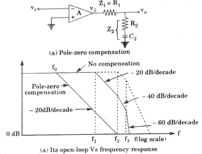
Q1. Explain pole-zero compensation method.
Ans. 1. In this method, both pole and zero are added to the uncompensated transfer function A.
2. Figure.(a) shows the circuit arrangement of the pole-zero compensation method. The zero is added at a higher frequency than the pole.
3. The transfer function of the compensation network is given by,
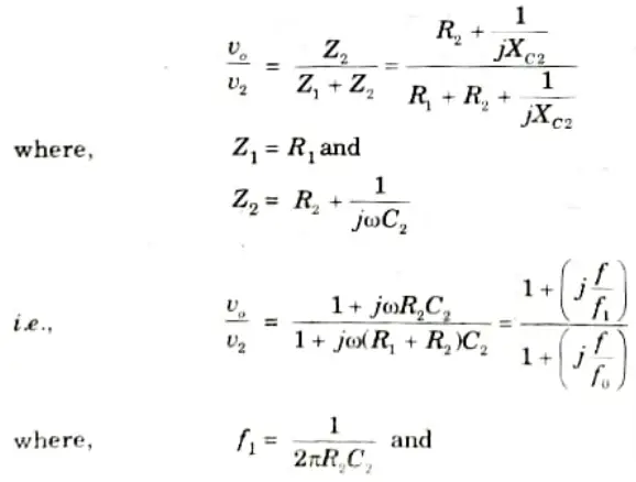
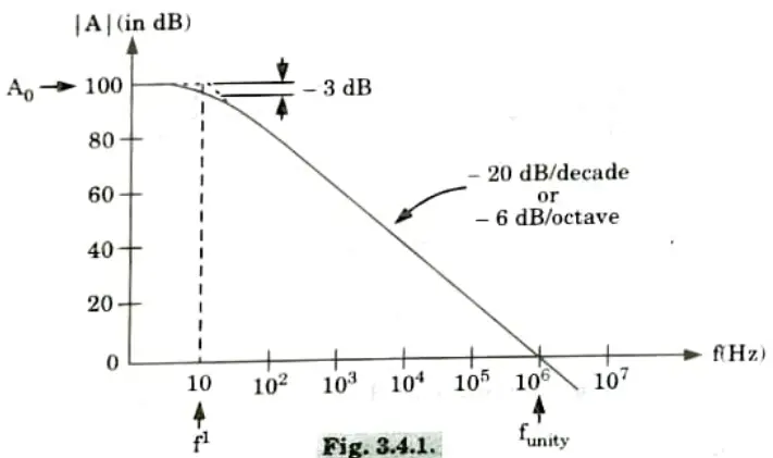
4. The compensating network introduces a zero at the first corner frequency f1 of uncompensated transfer function represented by A’, which cancels the effect of pole at f1.
5. The pole of the compensation network at fo given as

selected such that the compensated transfer function A’ passes through 0 dB at the second corner frequency f2. This is shown in Fig.(b) graphically by having A’ passing through 0 dB at frequency f2 with a slope of -20 dB/decade.
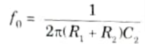
6. The overall transfer function of the amplifier with compensation network is given by
Q2. Write a short note on internal frequency compensation.
Ans.
- 1. In other applications, like instrumentation, a broad bandwidth may not be the essential need. Internally corrected Op-Amps, also known as compensated Op-Amps, can be used in these circumstances. They are discovered to be stable without any external compensatory techniques and irrespective of the closed-loop gain amount.
- 2. The frequency response of 𝝻A741 Op-Amp which is internally compensated is reproduced in Fig.
- 3. A 30 pF internal capacitance in the Op-Amp 741 shunts OFF the signal current at higher frequencies, causing the output signal to weaken.
- 4. The circuit’s stability is ensured by the internal compensating capacitor, which causes the open-loop gain to drop off at a rate of -20 dB/decade.
- 5. The gain-bandwidth (GBW) product of the Op-Amp 741 is 1 MHz. This indicates that at any point along the open loop gain Vs frequency curve, the product of gain and frequency is 1 MHz.
- 6. If the Op-Amp is connected for a gain of 60 dB, or 103, then the bandwidth obtainable is 1 KHz. For a gain of 10, the bandwidth increases to 100 KHz.
Q3. Describe the sample and hold circuit with the help of an Op-Amp. What are the applications of sample and hold circuit ?
Ans. A. Sample and hold circuit:
1. Fig. shows the circuit for sample and hold using Op-Amp. It samples an input signal and holds on to its last sampled value until the input is sampled again.
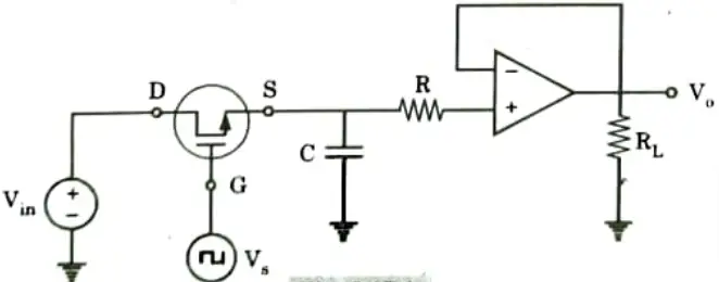
- 2. Op-Amp and enhancement MOSFET is used in the circuit. MOSFET acts as switch to control Vs while C serves as a storage clement. Vin, to be sampled is applied to drain and Vs across the gate of MOSFET.
- 3. During positive portion of Vs, the MOSFET conducts and allow input voltage to charge capacitor C.
- 4. When Vs is zero, the MOSFET is OFF and the discharge path for capacitor Cis through the Op-Amp.
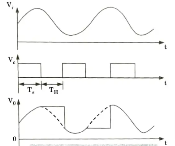
- 5. However, the input resistance of the Op-Amp voltage follower is also very high: hence the voltage across C is retained. Fig. shows the input and output waveforms.
- 6. The time period Ts of voltage Vs during which the voltage across the C is equal to the input voltage are called sample periods.
- 7. The time period TH of Vs during which the voltage across the capacitor C is constant are called hold periods as shown in Fig.
B. Applications:
- i. PAM demodulator.
- ii. PCM.
- iii. Analog to digital converters.
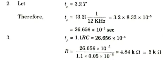
Q4. A monostable multivibrator is to be used as divide-by-4 network. The frequency of input trigger is 12 KHz. If the value of C = 0.05 𝝻F, what should be value of R?
Ans. Given: f = 12 KHz, C = 0.05 𝝻F
To Find: R.
1. For a divide-by-4 network, tp should be slightly larger than thrice the period of the input trigger signal.
Q5. What do you mean by the quadrant operation of multiplier? Draw and explain a GILBERT analog multiplier.
Ans. A. quadrant operation of multiplier:
- 1. The quadrant specifies whether the circuit can handle bipolar signals at its inputs.
- 2. The device in the first quadrant only accepts positive input signals, the device in the second quadrant accepts one bipolar signal and one unipolar signal, and the device in the fourth quadrant accepts two bipolar signals.
B. GILBERT analog multiplier:
1. The emitter coupled cell is modified into the GILBERT multiplier cell, which enables four-quadrant multiplication. It serves as the foundation for the majority of integrated circuit balanced multipliers.
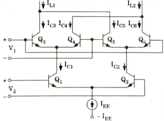
2. Two cross-coupled emitter-coupled pairs in series connection with an emitter coupled pair form the structure of the GILBERT multiplier cell.
3 The collector currents of Q3 and Q4 are given by
4. Similarly the collector currents of Q5 and Q6 are given by
5. The collector currents IC1 and IC2 of transistors, Q1 and Q2 can be expressed as
6. Substituting eq. (3.28.5) in eq. (3.28.1) and (3.28.2), we get
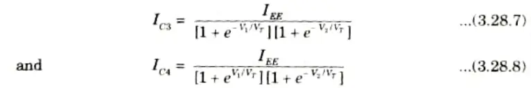
7. Similarly, substituting eq. (3.28.6) in eq. (3.28.3) and (3.28.4), we get
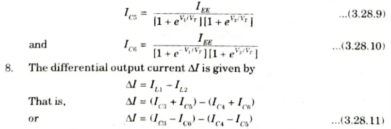
9. Substituting eq. (3.28.7) to (3.28.10) in eq. (3.28.11) and employing exponential formulae tor hyperbolic functions, we get
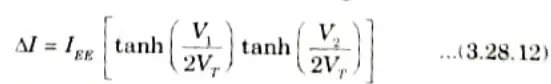
eq. (3.28.12) shows that when V1 and V2 are small, the GILBERT cell shown in Fig. can be used as a four-quadrant analog multiplier with the use of current-to-voltage converters.
Q6. Write a short note on logarithmic amplifier with its mathematical expression.
Ans. 1. A fundamental log amplifier is formed by placing a transistor in negative feedback path of Op-Amp as shown in Fig.
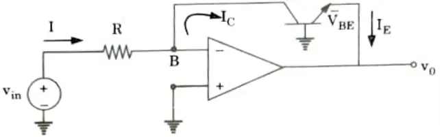
2. The node B is at virtual ground hence VB = 0. The current through resistorR can be written as
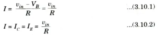
3. At the Op-Amp input current is zero

4. The voltage VCB = 0 as the collector is at virtual ground and base is grounded. Hence, we can write the equation of IC as,

5. Take natural log on both sides of eq. (3.10.4)
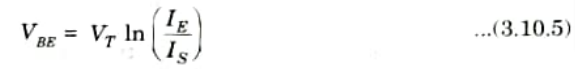
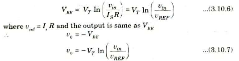
6. Substitute the eq. (3.10.2) in eq. (3.10.5), we get

Integrated Circuits Btech Quantum PDF, Syllabus, Important Questions
| Label | Link |
|---|---|
| Subject Syllabus | Syllabus |
| Short Questions | Short-question |
| Question paper – 2021-22 | 2021-22 |
Integrated Circuits Quantum PDF | AKTU Quantum PDF:
| Quantum Series | Links |
| Quantum -2022-23 | 2022-23 |
AKTU Important Links | Btech Syllabus
| Link Name | Links |
|---|---|
| Btech AKTU Circulars | Links |
| Btech AKTU Syllabus | Links |
| Btech AKTU Student Dashboard | Student Dashboard |
| AKTU RESULT (One VIew) | Student Result |