
With the help of Aktu Btech Quantum Notes, discover the world of integrated circuits. With the help of these crucial, often asked questions, you can master important subjects and ace your tests. Use them right away to succeed! Unit-1 The 741 IC Op-Amp
Dudes 🤔.. You want more useful details regarding this subject. Please keep in mind this as well.

Important Questions For Integrated Circuits:
*Quantum               *B.tech-Syllabus
*Circulars                *B.tech AKTU RESULT
* Btech 3rd Year    * Aktu Solved Question Paper
Q1. Write a short note on 741 Op-Amp circuit and discuss the bias circuit.
Ans. A. Op-Amp circuit:
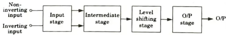
- 1. Generally BJT based Op-Amp is focused on 741 Op-Amp circuit. If we use IC design, the circuits use large number of transistors but relatively few resistors and only one capacitor.
- 2. The block diagram of typical Op-Amp is shown in Fig.
- 3. The equivalent circuit of Op-Amp is shown in Fig.
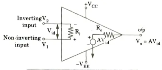
B. Characteristics of ideal Op-Amp:
- 1. Infinite voltage gain, Av = ∞.
- 2. Infinite input resistance, Ri = ∞.
- 3. Zero output resistance, Ro = 0.
- 4. Zero output voltage when input voltage is zero.
- 5. Infinite bandwidth.
C. Bias circuit:
- 1. The bias circuit is used to provide proportional current in the collector of transistor.
- 2. Some transistors form the current mirror, in which transistor collector provides bias current for other output stage of Op-Amp.
- 3. Finally some transistors works to provide the VBE drop between the bases of output transistors for proper functioning of the device.
Q2. Describe what is mean by output short circuit protection and explain how it is achieved in the output stage of IC 741.
Ans.
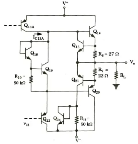
- 1. The short-circuit protection circuitry is shown in the Fig.
- 2. The Op-Amp 741 contains a number of transistors that are normally in the OFF state.
- 3. When the output terminal gets shorted to the ground, while keeping a positive output voltage due to certain input signal, this will induce a large current in the output transistor Q14.
- 4. This will result in producing heat and cause burn-out of the transistor. Therefore, when current flow in Q14 reaches 20 mA, voltage drop across R6 becomes 27 x 20 = 540 mV, which bias the transistor Q15.
- 5. Similarly, the maximum current in Q20 is limited by R7, Q21 and Q24.
- 6. When the current increases, the voltage drop across R7 becomes sufficient and the transistor Q21 becomes ON and Q21 and Q24 shunt the excess current away from the transistor Q20, hence protects the output transistor.
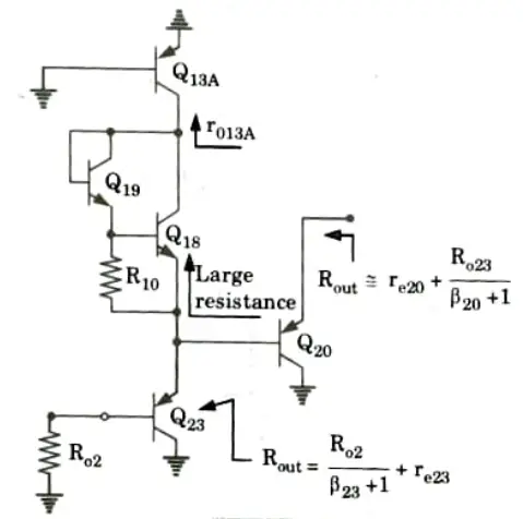
Output resistance of 741 Op-Amp:
- 1. The output resistance of the Op-Amp Rout is determined from the Fig. In accordance with the definition of Rout the input source feeding the output stage is grounded, but its resistance is included.
- 2. We have assumed that the output voltage vo is negative and thus Q20 is conducting most of the current; transistor Q14 has therefore been eliminated. The exact value of the output resistance will depend on which transistor (Q14 or Q20) is conducting and on the value of load current.
- 3. The resistance of emitter of Q23 is
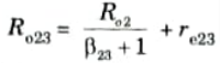
This resistance appears in parallel with the series combination of ro13A and the resistance Q18-Q19 network.
- 4. Since ro13A alone is larger than Ro23, the effective resistance between the base of Q20 and ground approximately to Ro23, the output resistance Rout as
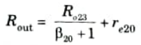
- 5. The output resistance of the 741 is specified to be typically 75𝝮.
Q3. Determine the small-signal model of the second stage of the 741 Op-Amp.
Ans. 1. Fig. shows the 741 second stage Op-Amp prepared for small-signal analysis. Now we analyze the second stage to determine the values of the parameters of the equivalent circuit shown in Fig.
a. Input resistance: The input resistance Ri2 can be found by

Substituting the appropriate parameter values yields Ri2 = 4 M𝝮.
b. Transconductance:
i. From the equivalent circuit of Fig. we see that the transconductance Gm2 is the ratio of the short-circuit output current to the input voltage.
ii. Short-circuiting the output terminal of the second stage to ground makes the signal current through the output resistance of Q13B zero, and the output short-circuit current becomes equal to the collector signal current of Q17(i17). This can be easily related to vi2 as follows:

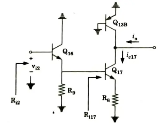
iii. These equations can be combined to obtain
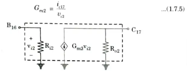
c.Output resistance:
i. To determine the output resistance Ro2 of the second stage in Fig. we ground the input terminal and find the resistance looking back into the output terminal.
ii. So, Ro2 is given by
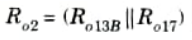
where Ro13B is the resistance looking into the collector Q13B while its base and emitter are connected to ground and Ro17 is the resistance looking into the collector of Q17.
Q4. Draw and explain the simplified model of 741 Op-Amp.
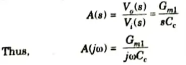
Ans. 1. Fig. shows a simplified model of the 741 Op-Amp. The gain of 2nd stage is assumed sufficiently large. The output stage is assumed to be ideal unity-gain follower.
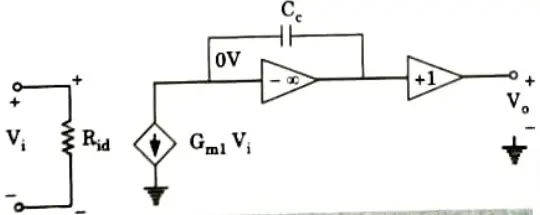
2. From the Fig.
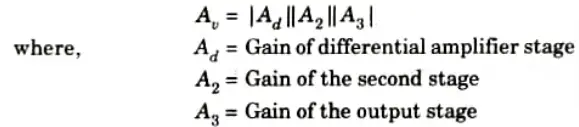
Q5. Find out the overall gain of an Op-Amp Ic-741 giving its cascaded equivalent circuit derived for its three stages. Also derive the relationship between ft and slew rate for IC-741.
Ans. A. Overall gain of an Op-Amp IC-741:
The overall voltage gain Av of the Op-Amp is the product of voltage gains of each stage as given by,
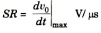
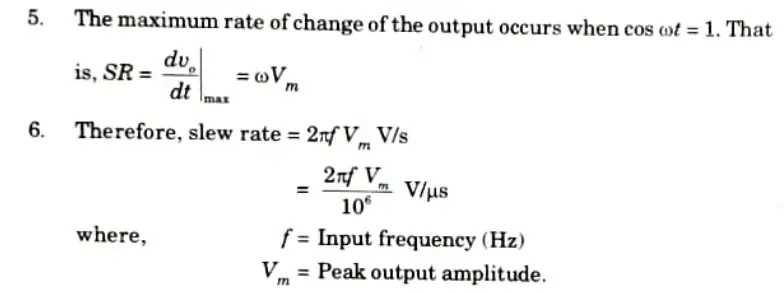
B. Slew rate: The slew rate is defined as the maximum rate of change of output voltage per unit of time and is expressed in volts per microsecond, i.e.,
C. Relationship between ft and SR:
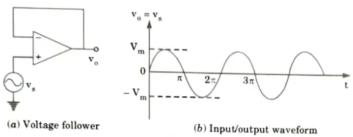
1. Consider a voltage follower shown in Fig.(a). The input is large amplitude, high frequency sine wave.
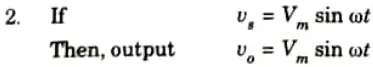
3. Fig.(b) shows the input-output waveform.
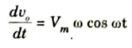
4. The rate of change of the output is given by,
Q6. Draw and explain the frequency response of IC 741.
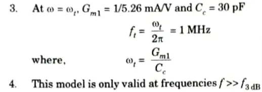
Ans. 1. The system employs the Miller compensation technique.
2. A capacitor (Cc) of about 30 pF is connected in the negative feedback path of the second stage.
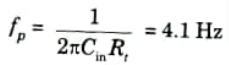
3. An estimation of frequency of poles can be obtained as,
Since, this value of capacitor is large so we neglect all other between capacitances the base and ground of transistor.
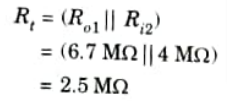
5. The total resistance,
6. The dominant pole has a frequency fp,
7. Calculate all the values of poles and a bode plot is shown in Fig.

where, ft is unity-gain bandwidth.
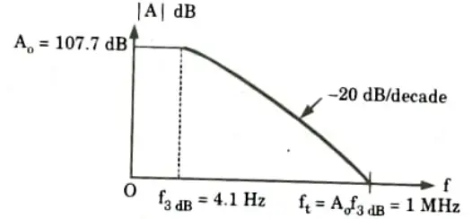
9. Bode plot signifies that the phase shift at ft is – 90° and thus margin phase is 90°. This phase margin is sufficient to provide stable operation of closed-loop amplifiers with any value of feedback factor 𝝱.

Integrated Circuits Btech Quantum PDF, Syllabus, Important Questions
| Label | Link |
|---|---|
| Subject Syllabus | Syllabus |
| Short Questions | Short-question |
| Question paper – 2021-22 | 2021-22 |
Integrated Circuits Quantum PDF | AKTU Quantum PDF:
| Quantum Series | Links |
| Quantum -2022-23 | 2022-23 |
AKTU Important Links | Btech Syllabus
| Link Name | Links |
|---|---|
| Btech AKTU Circulars | Links |
| Btech AKTU Syllabus | Links |
| Btech AKTU Student Dashboard | Student Dashboard |
| AKTU RESULT (One VIew) | Student Result |