
Aktu Btech Quantum Notes will help you unlock the realm of integrated circuits. Utilise these crucial, commonly asked questions to master vital concepts and ace your tests. For success, use these right away! Unit-2 Linear Applications of IC Op-Amp
Dudes 🤔.. You want more useful details regarding this subject. Please keep in mind this as well.

Important Questions For Integrated Circuits:
*Quantum               *B.tech-Syllabus
*Circulars                *B.tech AKTU RESULT
* Btech 3rd Year    * Aktu Solved Question Paper
Q1. Draw and explain I-V and V-I converters and derive its output.
Ans. A. I-V converter:
1. The current to voltage converter is shown in Fig.
2. The open-loop gain Av of the Op-Amp is very large, so due to virtual short concept,

3. As the input impedance of Op-Amp is very high,
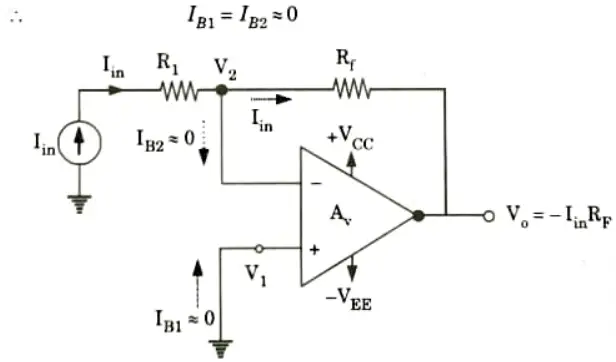
4. Gain of inverting amplifier is given by
5. Thus the inverting terminal is also at ground potential and entire input voltage appears across R1.
6. Substituting eq. (2.2.2) in eq. (2.2.1), we get
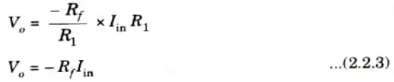
7. The eq. (2.2.3) shows how this circuit converts input current into a proportional voltage.
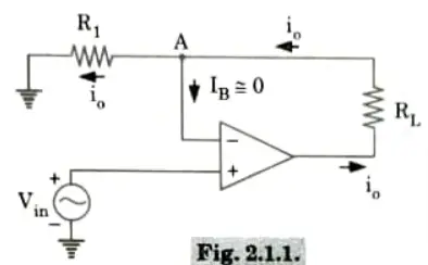
B. V-I converter:
1. The Fig. shows an arrangement of voltage to current converter with load resistor RL. Here RL is in floating condition i.e., not connected to ground.
2. The input is applied to non-inverting end and the feedback voltage across R1 drives the inverting input end.
3. The feedback voltage across R1 depends on the output current io and it is in series with the input difference voltage Vid.
4. Due to the concept of virtual ground, the voltage at node A will be Vin.

i.e., an input voltage Vin is converted into an output current of Vin/R1.
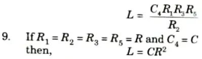
Q2. Describe the Antoniou inductance simulation circuit with properly labeled circuit diagram and give mathematical expressions in support of your answer.
Ans. 1. Fig. shows the Antoniou inductance simulation circuit.
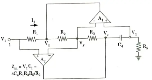
2. Applying KCL, we get
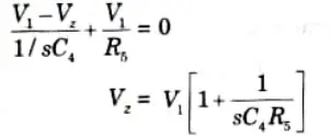
3. Apply KCL, we get
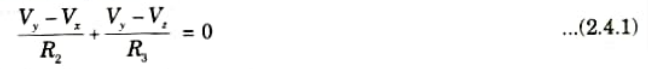
4. Substituting the value of Vz in eq. (2.4.1)
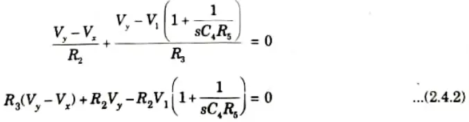
5. Apply KCL, then we get
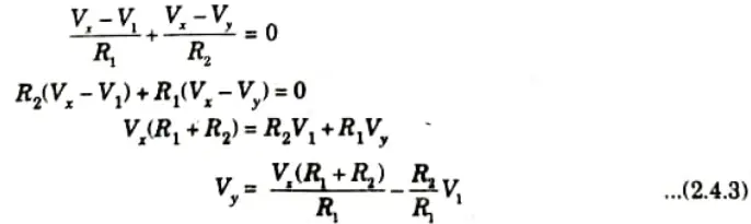
6. Now put the value of Vy in eq. (2.4.2),
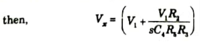
7. Current across resistance R1,
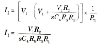
8. Then input impedance
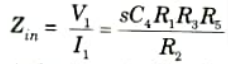
which is that of an inductance L given by,
Q3. Classify Active filters and write its advantages.
Ans. A. Classification of active filters:
- 1. Active filters employ transistors or Op-Amps in addition to resistors and capacitors.
- 2. The type of element used dictates the operating frequency range of the filter. The classification of active filter is shown in Fig.
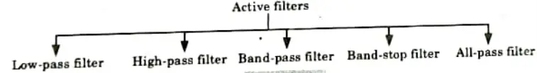
- 3. Each of these filters uses an Op-Amp as the active element and resistors and capacitors as the passive elements.
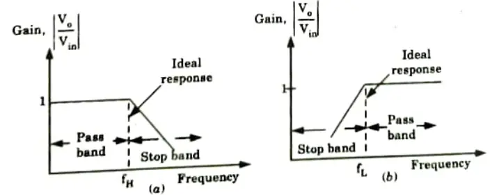
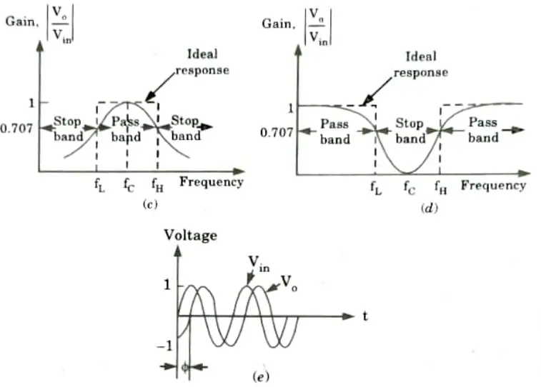
- 4. Fig. shows frequency response characteristics of the five types of filters. The ideal response is shown by dashed curves, while the solid lines indicate the practical filter response.
B. Advantages of active filters:
- 1. No loading problem: High input resistance and low output resistance are provided by the Op-Amp. Op-Amp active filters do not load the input source or load, as a result.
- 2. Flexibility in gain and frequency adjustment: Active filters offer gain flexibility because the input signal is not attenuated while travelling through the filter. Moreover, the active filter is simple to tune, making frequency change simple.
- 3. Small component size: Active filters use components which are smaller in size.
- 4. No insertion loss: The active filters do not exhibit any insertion loss.
- 5. Passband gain: These filters provide some pass band gain.
Q4. Write a short note on higher-order filter.
Ans. 1. First-order filters change their gain in the stopband at a rate of 20 dB per decade, while second-order filters change their gain at a rate of 40 dB per decade. This indicates that the real stopband response of the filter approaches its ideal stopband characteristic as the filter’s order is raised.
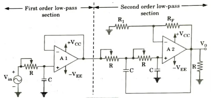
- 2. Higher-order filters, such as third, fourth, fifth, and so on, are formed simply by using the first and second-order filters.
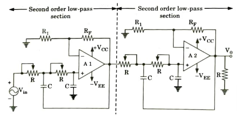
For example, a third-order low-pass filter is formed by connecting in series or cascading first-and second-order low-pass filters; a fourth-order low-pass filter is composed of two cascaded second-order low-pass sections, and so on.
- 3. Although there is no limit to the order of the filter that can be formed, as the order of the filter increases, so does its size.
- 4. Its accuracy also decreases because, as the order of the filter increases, the discrepancy between the real stopband response and the theoretical stopband response grows.
- 5. The third- and fourth-order low-pass Butterworth filters are shown in Fig. The voltage gain of the first-order portion is one and that of the second-order section is two in the third-order filter.
- 6. In the fourth order, the first section’s gain is 1.152, but the second section’s gain is 2.235. These gain values must remain constant regardless of the filter’s cut-off frequency in order to ensure Butterworth response.
- 7. Furthermore, the overall gain of the filter is equal to the product of the individual voltage gains of the filter sections. Thus the overall gain of the third-order filters is 2.0, and that of the fourth order filters is (1.152) (2.235) = 2.57.
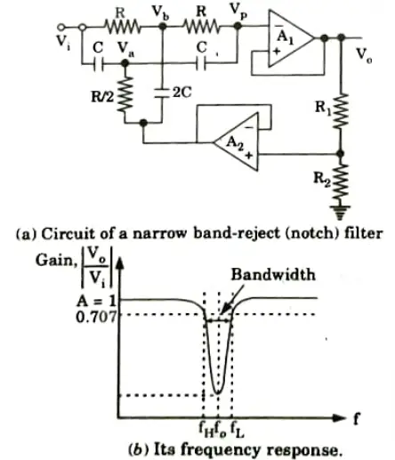
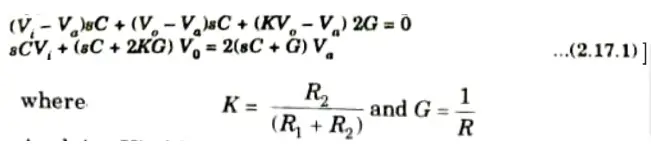
Q5. Draw and explain narrow band-reject filter. Also, find its transfer function.
Ans. A. Band-reject filter:
The stopband frequencies are attenuated by the band-reject filter, also known as the band-elimination or band-stop filter, and are passed outside of this band.
B. Types:
i. Narrow band-reject filter:
1. The narrow band-reject filter, often called the notch filter, is the twin T network cascaded with the voltage follower as shown in Fig.(a).
2. Applying Kirchhoff’s current law at node Va, we get
3. Applying Kirchhoff current law at node Vb, we get
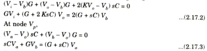
4. From the above three node voltage eq. (2.17.1), (2.17.2) and (2.17.3), the transfer function can be written as
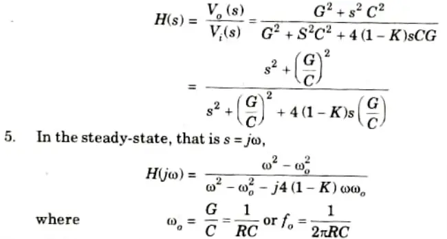
6. At 3 dB cut-off frequency,
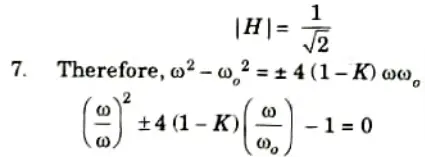
8. Upon solving the above quadratic equation, we obtain the upper and lower half power frequencies as,
9. The 3 dB bandwidth is
ii. Wide band-reject filter:
1. Fig.(a) shows a wide band-reject filter that is obtained by paralleling a high-pass filter with a cut-off frequency of fL with a low-pass filter.
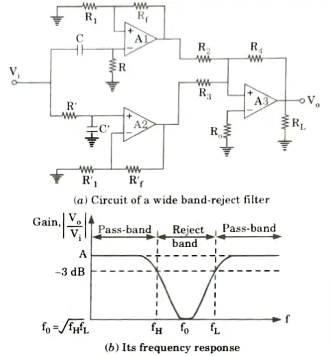
2. With cut-off frequency of fH, provided fL:> fH and a summing amplifier connected in series to add the filtered individual passband components.
3. The passband gains of both the high-pass and low-pass sections must be equal.
4. The frequency response characteristic of the wide band-reject filter is shown in Fig.(b).
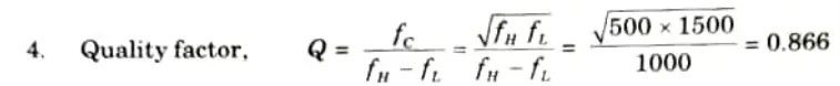
Q6. Design a wide bandpass filter with fL = 500 Hz and fH = 1500 Hz and passband gain of 5, draw frequency response of the filter and find value of Q.
Ans.Given: fL = 500 Hz; fH = 1500 Hz; A = 5
To Find: Q.
A. Components of the low-pass filter:
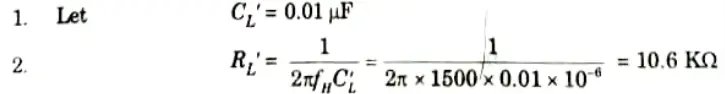
3. The gain of the low-pass filter can be considered half,
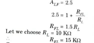
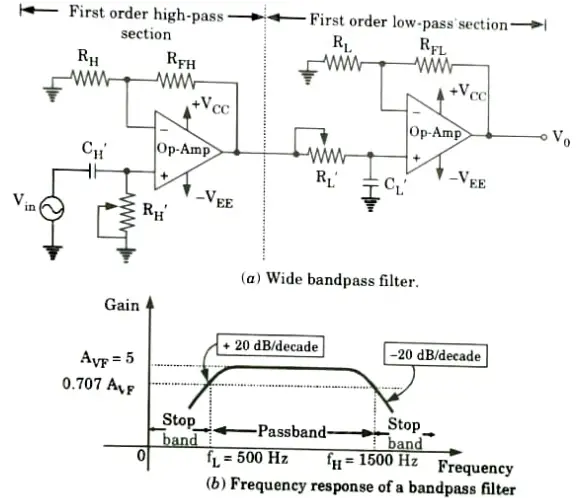
B. Components of the high-pass filter:

Integrated Circuits Btech Quantum PDF, Syllabus, Important Questions
| Label | Link |
|---|---|
| Subject Syllabus | Syllabus |
| Short Questions | Short-question |
| Question paper – 2021-22 | 2021-22 |
Integrated Circuits Quantum PDF | AKTU Quantum PDF:
| Quantum Series | Links |
| Quantum -2022-23 | 2022-23 |
AKTU Important Links | Btech Syllabus
| Link Name | Links |
|---|---|
| Btech AKTU Circulars | Links |
| Btech AKTU Syllabus | Links |
| Btech AKTU Student Dashboard | Student Dashboard |
| AKTU RESULT (One VIew) | Student Result |