Here we are discussing for All Short Question In Digital System Design B.Tech AKTU 2022-23. Hope This Blog will Help you in your upcoming Exams.
Dudes 🤔.. You want more useful details regarding this subject. Please keep in mind this as well.

Important Questions For Digital System Design:
*Unit-01     *Unit-02
*Unit-03    *Unit-04
*Unit-05    *Short-Q/Ans
*Question-Paper with solution 21-22
UNIT:01 – Logic Simplification and Combinational Logic Design
1. Define combinational circuits.
Ans Input variables, logic gates, and output variables make up the system. Logic gates produce output signals by accepting signals from input variables. Through this procedure, binary information is converted from input data to the desired output data.
2. Write the difference between combinational and sequential circuits.
| Combinational circuits | Sequential circuits |
|---|---|
| It consists of interconnection of logic gates only | It consists of storage elements and logic gates. |
| Output of combinational circuits depends only on the present value of input. | Output of sequential circuit depends on present and previous value of input and output. |
3. In how many ways the binary codes are classified ?
Ans
- 1. Weighted codes
- 2. Non-weighted codes
- 3. Reflective codes
- 4. Sequential codes
- 6. Alphanumeric codes
- 6. Error detecting and correcting codes.
4. Define cyclic codes.
Ans These codes are referred to be cyclic codes when the bit pattern of two consecutive numbers differs by just one bit position.
5. Write the advantages of Gray code over the straight binary number sequence.
Ans.
1. The Gray code is employed in applications where the regular flow of binary numbers produced by the hardware could result in a mistake or ambiguity when moving from one number to the next. Since only one bit changes value during the transition between two numbers, the Gray code solves this issue.
2. Gray coding uses a shaft’s angular position to continuously shift to represent analogue data. Gray code removes any doubt regarding the relationship between the shaft’s angle and the sensor’s encoded value.
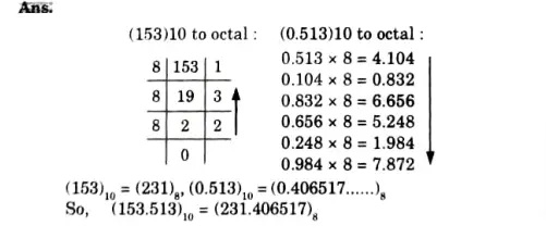
6. Convert (153.513)10 to an octal number?
7. Write four advantages of digital systems over analog systems.
Ans
- 1. Digital communication systems are more reliable than analogue ones because they can withstand signal degradation caused by channel noise much better.
- 2. Digital hardware implementation in a digital communication The system is adaptable and allows for the use of digital switching, microprocessors, etc.
- 3. Multiple digital signals can be multiplexed together in a digital system to make better use of the available bandwidth.
- 4. Large data sets may be stored with ease in a digital system.
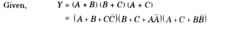
8. Convert the following expression into canonical POS form

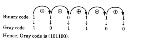
9. Convert the binary number (1 1 0111)2 into Gray code.
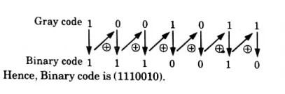
10. Convert gray code 1001011 to binary.
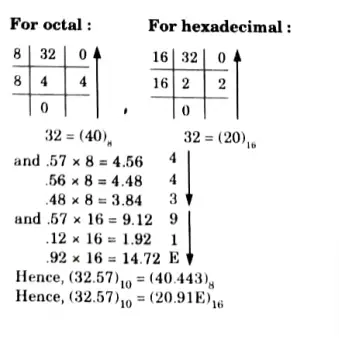
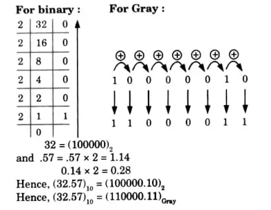
11. Convert the decimal number 32.57 in octal, binary, hexadecimal and Gray.
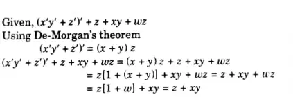
12. Simplify the following boolean expression to a minimum number of literals: (*’y +zY +z+*y +wz
13. Convert the following
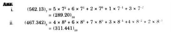
i. (562.13)7= (7)10
ii. (467.342)8= (?)10
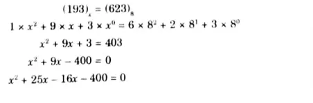
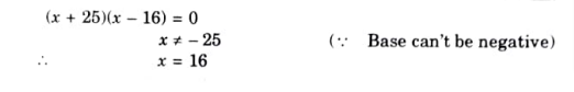
14. Determine the value of base x, if (193)X = (623)8
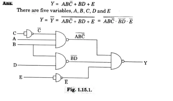
15. Implement the expression Y= AB + BD + E using NAND gate only.
UNIT:-02 (MSI Devices)
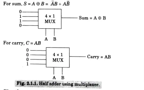
1. Design a half adder using a multiplexer.
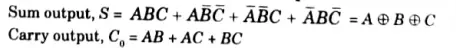
2. Give the expression of full adder output.
3. Draw the logic diagram of half subtractor.

4. Explain multiplexer circuit.
Ans Combinatorial circuit that chooses a binary signal from among several input lines and sends it to a single output line. A group of selection lines determine which input line will be chosen. The bit combination on the 2N input lines and n choose lines determines which input is chosen.
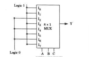
5. Implement the following function using 8 x 1 MUX, Y (A,B, C) = Σm(0, 1,3,5, 7).
6. Give the circuit diagram and output equation for 4×1 MUX.

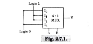
7. Implement the following expression using 4: 1 MUX
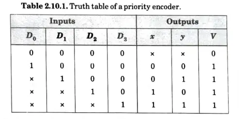
8. What do you mean by priority encoder?
Ans The priority function is a part of the encoder circuit. When two or more inputs are equal to 1 at the same time, the priority encoder operates so that the input with the highest priority takes precedence.
9. Which circuit is used at input of a communication system ?
Ans Encoder is used at input of communication systems.
10. Specify the purpose of a valid bit indicator in priority encoder.
Ans: When one or more inputs are equal to 1, the valid bit indicator in the priority encoder is set to 1. There is no valid input if all of the inputs are 0, and a valid bit indication is equal to 0. When the valid bit indication is set to 0, the other two outputs are specified since I don’t care about the requirements and are not examined.
11. What are the circuits by which all the expressions are implemented?
Ans All boolean expressions are implemented using a multiplexer or a decoder.
12 Write the difference between decoder and demultiplexer.
| Decoder | Demultiplexer |
|---|---|
| It has n input line | It has 1 input line |
| Enable line is present | There is no enable line. |
| There is no select line. | Select line is present |
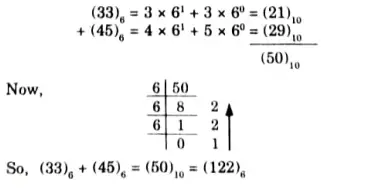
13. What is (33)6 + (45)6
UNIT:-03 (Sequential Logic Design)
1. Define sequential circuits.
Ans A combinational circuit with storage elements attached to create a feedback route makes up a sequential circuit.
2. What do you mean by flip-flops?
Ans Flip-flops are storage components that are managed by a clock transition. It is a binary storage system that can hold just one bit of data. Flip-flops are gadgets that are edge triggered.
3. Give the major differences between latch and flip-flop.
| Latch | Flip-flop |
|---|---|
| Storage element that operates with signal levels. | Storage element that are controlled by clock transition. |
| It is level triggered | It is edge triggered. |
| There is no clock pulse | There is a clock pulse |
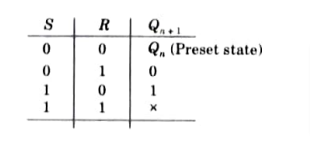
4. Give the function table of SR latch.
5. Draw Master-Slave flip-flop.
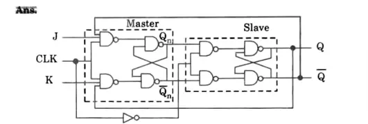
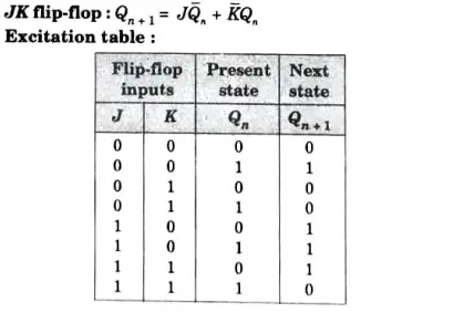
6. Express the characteristic equation for the JK flip-flop.
OR
Write the excitation table and characteristic equation of JK flip-flop.
7. Define shift registers.
ANS. With the use of clock pulses, binary data in a register can be transferred from one flip-flop to another inside the register or outside of it. Shift registers are the registers that permit these data transfers.
8. Give the classification of shift register on the basis of mode of operation.
Ans
- 1. Serial in serial out shift register (SISO)
- 2. Serial in parallel out shift register (SIPO)
- 3. Parallel in serial out shift register (PIS0)
- 4. Parallel in parallel out shift register (PIPO)
9. Give the application of the shift register.
Ans Shift register are used in many application as:
1. Time delay 2. Serial to parallel data converter
3. Parallel to serial data converter
10. What is the counter ?
Ans A sequential logic circuit known as a counter is able to count the number of clock pulses that enter its clock input. This count sequence could be nonsequential, ascending, or falling. The counter output displays a specific order of states.
11. Define asynchronous counter or ripple counter.
Ans A complementary sequence of flip-flops are coupled together to form a binary asynchronous/ripple counter, with the output of each flip-flop being connected to the clock input of the subsequent higher-order flip-flop. The incoming clock pulses are received by the flip-flop that is holding the least significant bit.
12. Define synchronous counter.
Ans The synchronous counter, also known as a parallel counter, is one in which every flip-flop is activated simultaneously by the clock pulse. An asynchronous counter’s delay may be reduced using a synchronous counter.
13. What is the modulus of a counter ?
Ans. The modulus of the counter is the number of states that the counter went through before returning to its initial state.
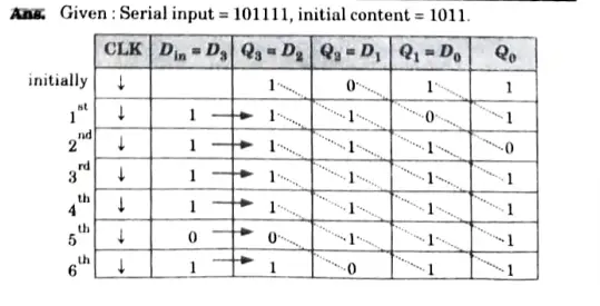
14. The contents of a four bit register are initially 1011. The register is shifted six times to the right with serial input being 101111. What are the contents of the register after each shift?
15. How many flip-flops are required to design Mod-5 ring counter and Mod-5 Johnson counter?
Ans. Mod-5 Ring counter 5 Flip-flop.
Mod-5 Johnson counter 3 Flip-flop.
16. What are the required numbers of flip-flops in a MOD-16 asynchronous counter, MOD-16 synchronous counter,MOD-16 Johnson counter ?
Ans
MOD-16 asynchronous counter :4 flip-flop required
MOD-16 synchronous counter :4 flip-flops required
MOD-16 Johnson counter 8 flip-flops required.
17. What is race around condition?
Ans An asynchronous sequential circuit is said to have a race-around condition when two or more binary state variables change their value in response to an input variable change. By utilising a master-slave JK flip-flop, it is removed.
UNIT:-04 (Logic Families and Semiconductor Memories)
1. What do you mean by bipolar and unipolar logic families?
Ans
Bipolar logic family : Due to the fact that both electrons and holes are charge carriers, current flows in this family of logic.
Unipolar logic family: It consists of n-channel metal oxide field-effect transistors (NMOS), CMOS, and p-channel metal oxide semiconductor field-effect transistors (PMOS). Any one sort of carrier can be the cause of the current flow.
2. What are the uses of the ECL family ?
Ans Applications requiring very high frequencies are used when the ECL family’s speed is higher. It is utilised in lightning-fast computers and extremely quick specialised applications.
3. What is the difference between CMOS gate and TTL gate?
Ans 1. TTL and ECL gates are essentially unidirectional, whereas CMOS gates can carry signals in both directions.
2. CMOS consists of n-MOS and p-MOS but TTL and ECL use transistors.
4. What do you mean by fan-out and fan-in ?
Ans Fan-out: The greatest number of standard loads that a logic gate’s output may drive without compromising normal operation is known as the fan-out of the gate. The loading factor is another name for fan-out.

Fun-in: The number of inputs that a logic gate is intended to handle is referred to as the fan-in.
5. What do you understand about noise margin?
Ans A logic circuit’s capacity to withstand noise voltages at its inputs is referred to as noise immunity. Noise margin is a metric used to assess noise immunity.
6. What is memory ?
Ans. A memory unit is a device from which information is retrieved when needed for processing and from which binary information is sent for storage. A memory is a set of cells that can store a significant amount of binary data.
7. What do you mean by FPGA ?
Ans A high capacity PLD is an FPGA (Field Programmable Gate Array). An FPGA’s gate array can be programmed by the user rather than the device’s creator for a specific purpose.
8. Write the steps that must be taken for the purpose of transferTing a new word to be stored into memory.
Ans The steps that must be taken for the purpose of transferring a new word to be stored into memory are as follows:
- 1. Apply the chosen word’s binary address to the address lines.
- 2. Apply the required data bits to the data input lines so that they can be stored in memory.
- 3. Activate the write input.
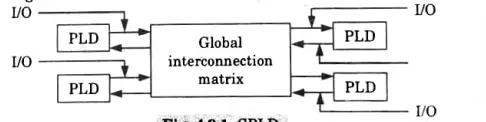
9. What do you mean by CPLD ?
Ans The term “complex-programmable logic device” (CPLD) refers to a group of PLD blocks that are connected by a global interconnection matrix at both their input and output.
10. How many address lines and data V0 lines are required for a 16K x 12 memory ?
ANS

11. Define memory read and write operation.
Ans Memory write operations and memory read operations are terms used to describe the processes of adding new information to memory and retrieving previously stored information from memory.
12. What is ROM ?
Ans In a digital system, read-only memory is a type of memory that can only be utilised for reading data. This implies that pertinent binary data is already present in memory and is accessible at any time for retrieval or reading. However, writing cannot change that information. Non-volatile memory is ROM.
13. Define the random access memory (RAM).
Ans: The name “random access memory” (RAM) refers to a memory that can do both read and write operations and that always takes the same amount of time to transfer data to or from any desired random place. Volatile memory is RAM.
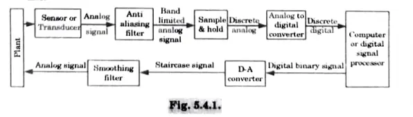
UNIT:-05 (D/A and A/D Converter)
1. Define D/A conversion.
Ans It involves translating a value encoded in digital form into a voltage or current that is proportional to the digital value.
2. What are the characteristics of D/A converter ?
Ans
- Resolution
- Accuracy
- Temperature sensitivity
- Linearity
- Settling time
3. What is the disadvantage of DAC ?
Ans The large range of resistor values needed is a drawback of binary weighted type DACs. It can be seen that longer input binary words are needed for higher resolution. As a result, the range of resistance value grows together with the amount of bits.
4. Draw the circuit diagram of AD and DWA converter.
5. Name the different types of ADCs used.
Ans
- 1.Flash (comparator) type converter
- 2. Counter type converter
- 3. Tracking or servo type converter
- 4.Successive approximation type comparator
6. Write the application in which integrating type converter is used ?
Ans
1. Digital meter
2. Panel meter
3. Monitoring systems where the conversion accuracy is critical.
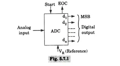
7. Draw the functional diagram of ADC and define its two additional control lines.
Control lines:
1. The START input to tell the ADC when to start the conversion.
2. The EOC output to announce when the conversion is complete
Functional diagram:
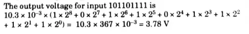
8. The basic step of a 9-bit DAC is 10,.3 mV. If0000o0000 represents 0V, what output is produced if the input is 101101111?
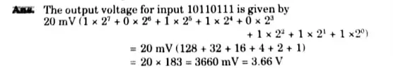
9. The basic step of an 8-bit DAC is 20 mV. If 00000000 represents OV, what is represented by the input 10110111?
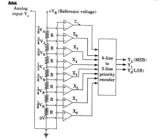
10. Draw the circuit diagram of the flash type A/D converter.
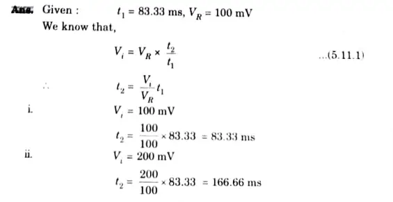
11. For a dual slope ADC, t1 is 83.33 ms and the reference voltage is 100 mV. Calculate t2 if Vi is
I. 100 mV and
ii. 200 mV.

Digital System Design Quantum, Syllabus, Important Questions
| Label | Link |
|---|---|
| Subject Syllabus | Syllabus |
| Short Questions | Short-question |
| Important Unit-1 | Unit-1 |
| Important Unit-2 | Unit-2 |
| Important Unit-3 | Unit-3 |
| Important Unit-4 | Unit-4 |
| Important Unit-5 | Unit-5 |
| Question paper – 2021-22 | 2021-22 |
Digital System Design Quantum PDF: | AKTU Quantum PDF:
| Quantum Series | Links |
| Quantum -2022-23 | 2022-23 |
AKTU Important Links | Btech Syllabus
| Link Name | Links |
|---|---|
| Btech AKTU Circulars | Links |
| Btech AKTU Syllabus | Links |
| Btech AKTU Student Dashboard | Student Dashboard |
| AKTU RESULT (One VIew) | Student Result |
1 thought on “Short Question – Digital System Design | AKTU B.tech Important Questions”