
In this Blog we are explore the Top 5 important Question in Digital System Design AKTU B.tech.
Here we are focusing only Unit 04 Logic Families and Semiconductor Memories. Hope this blog will help you for your upcoming exams.
Dudes 🤔.. You want more useful details regarding this subject. Please keep in mind this as well.

Important Questions For Digital System Design:
*Unit-01     *Unit-02
*Unit-03    *Unit-04
*Unit-05    *Short-Q/Ans
*Question-Paper with solution 21-22
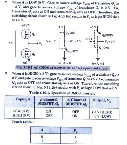
Q1.Describe the circuit and performance of CMOS inverter and state the characteristics of CMOS.
Answer
CMOS inverter:
1. It is made up of an NMOS transistor and a PMOS transistor, respectively. Both devices’ gates and drains are connected to the input, and both devices’ drains are connected to the output. The sources of PMOS transistor Q2 are connected to the positive supply voltage, whereas the sources of transistor Q1 are grounded.

Que 2. Discuss the concept of field programmable gate array FPGA). Describe the various structures of FPGA.
Answer
Field Programmable Gate Array:
1. FPGA is a powerful PLD (programmable logic device). An FPGA’s gate array can be programmed by the user rather than the device’s creator for a specific purpose.
2.Three programmable (configurable) logic modules (LMs) make up an FPGA: input and output blocks, switching matrix for connectivity, and configurable logic blocks (CLBs).
3. Combinational logic arrays, data multiplexers (MUX), and flip-flops make up the CLUB. Using a look-up table, the combinational array function is carried out (LUT).
Structures of FPGA:
i Programmable logic structure:
1. A two-dimensional array of CLBs makes up the programmable logic structure of an FPGA.
2. To enable the implementation of sequential logic, each CLB typically has one or two flip-flops.
3. Large designs are divided up and mapped to a variety of CLBs, each of which is configured (programmed) to carry out a certain task.
4. The goal design is then fully implemented by connecting these CLBs.
ii Programmable routing structure:
1. ClLB may be connected to FPGA in a variety of ways thanks to its three configurable routing resources.
2. Wires of varying lengths make up the vertical and horizontal routing channels, which can be joined together as needed.
3. These channels run vertically and horizontally between columns and rows of CLBs as shown in Fig. 4.16.1.
4. Input and output pins of CLBs can be connected to wires of either vertical or horizontal routing channels using connection boxes, which are a collection of programmable links.
5. At the point where the vertical and horizontal channels converge are switch boxes.
6. Wire segments in the horizontal and vertical channels can be connected using this group of programmable links.
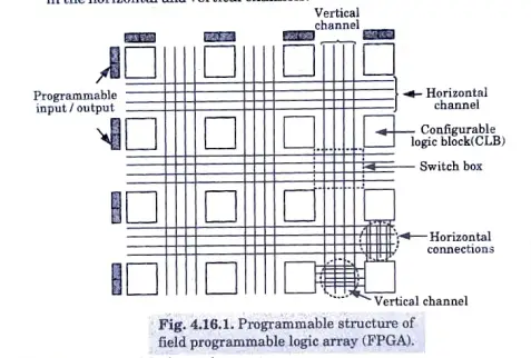
Programmable structure of field programmable logic array (FPGA).
iii. Programmable input/output:
1. As seen in Fig. 4.16.1, the majority of these are buffers that can be set up as input buffers, output buffers, or input/output buffers.
2. These enable the FPGA chip’s pins to serve as input, output, or input/output pins, respectively.
iv. Configurable logic blocks:
1. An FPGA contains a number of CLBs arranged in an array of rows and columns. Common row/column programmable interconnects link the logic blocks to the VO blocks.
2. The common row/ column interconnects are known as global interconnects.
3. A logie block is made up of several LMs. The fundamental logic units in an FPGA are called LMs. Local programmable interconnects are used to connect the LMs in a CLB.
Logic module:
1.A logie module (LM) consists of a LUT, a D-type fip-flop and a MUX. Most of the FPGAs are based on 4-input LUT. Fig. 4.16.2 shows a block diagram of a LM with 4-input LUT.
2. Either directly or via a D-type flip-flop, the output of the LUT is converted to the output of the LM. By using a flip-flop, the output can be set up for combinational or registered use.
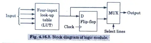
Block diagram of logic module
Que 3. What is the basic architecture of a PLA ? How is the capacity of a PLA specified ? How is it programmed? Explain.
| OR |
Write a short note on PLA.
| OR |
Write down the classification of semiconductor memories. Draw and explain the programmable logic array (PLA).
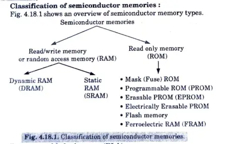
Classification of semiconductor memories
Programmable logic array (PLA) :
1.The mapping of irregular combinational function into regular structures is done via PLAs. The PLAN gives the designer a structured method for putting sum-of-product output functions with n variables into practise.
2.One common macro used in the implementation of FSM is PLA (finite state machine). Without requiring significant layout or design changes, the PLA’s functionalities can be altered significantly. Its nature is more condensed. Any logical operation can be described using SOP or POS.
3.PLA can be implemented in several forms, i.e., NOR-NOR, NAND-NAND, NAND-NOR.
4. FIG. 4.18.2 depicts the PLA’s internal logic, which has three inputs and two outputs. FIG. 4.18.3 depicts the PLA’s external logic.
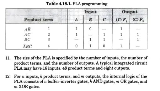
5. The particular boolean functions implemented in the PLAY of Fig. 4.18.3, are
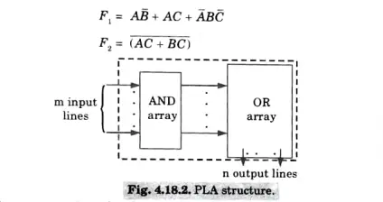
PLA structure.
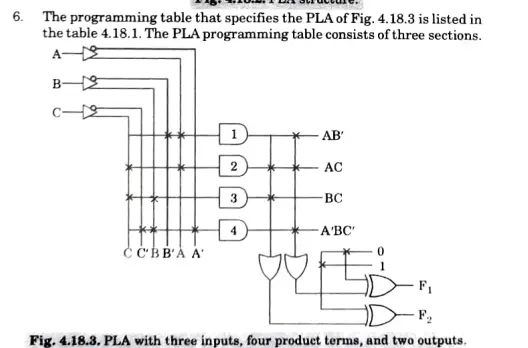
PLA with three inputs, four product terms, and two outputs.
7.The product phrase is listed numerically in the first part. The required pathways between input and AND gates are described in the second section. The route between the AND and OR gates is described in the third section.
8.We may have a T (true) or C (complement) for each output variable to use when programming the XOR gate.
9. For each product term, the inputs are narked with 1, 0 or- (dash).
10.The matching input variable is denoted with a 1 if the product term variable appears in the form in which it is true. If it appears complemented, a 0 is placed next to the appropriate input variable. The variable is indicated with a dash if it is not present in the product phrase.
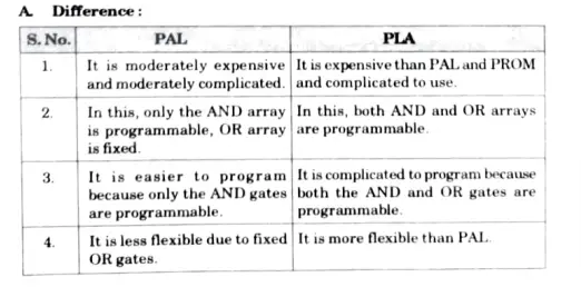
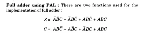
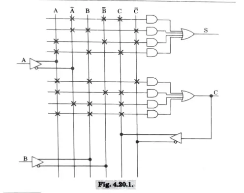
Que 4. Differentiate between PLA and PAL. Realize the full adder circuit using PAL.
B. Full adder using PAL:
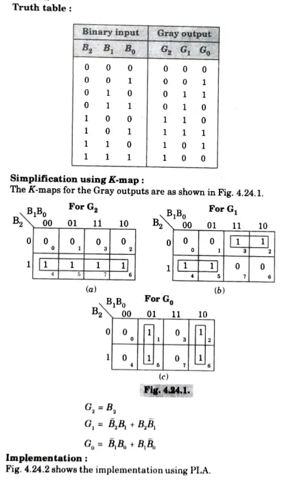
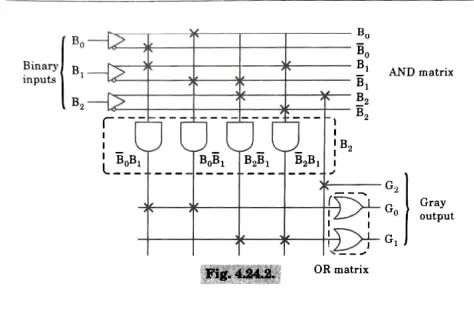
Que 5. Design a 3-bit binary to Gray code converter using PLA.
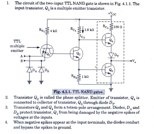
Q6.Describe the construction and operation of TTL NAND gate.
| OR |
Draw and explain the operation of a TTL NAND gate.
Answer
1. The circuit of the two-input TTL NAND gate is shown in Fig. 4.1.1. The input transistor, Q1 ís a multiple emitter transistor.
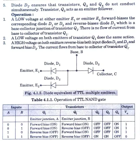
Diode equivalent of TTL multiple emitters

Digital System Design Quantum, Syllabus, Important Questions
| Label | Link |
|---|---|
| Subject Syllabus | Syllabus |
| Short Questions | Short-question |
| Important Unit-1 | Unit-1 |
| Important Unit-2 | Unit-2 |
| Important Unit-3 | Unit-3 |
| Important Unit-4 | Unit-4 |
| Important Unit-5 | Unit-5 |
| Question paper – 2021-22 | 2021-22 |
Digital System Design Quantum PDF: | AKTU Quantum PDF:
| Quantum Series | Links |
| Quantum -2022-23 | 2022-23 |
AKTU Important Links | Btech Syllabus
| Link Name | Links |
|---|---|
| Btech AKTU Circulars | Links |
| Btech AKTU Syllabus | Links |
| Btech AKTU Student Dashboard | Student Dashboard |
| AKTU RESULT (One VIew) | Student Result |