
The most commonly asked question in digital system design is covered in this blog post. concentrating on D/A and A/D Converter in Unit 05. I hope this blog will be useful for your examinations.
Dudes 🤔.. You want more useful details regarding this subject. Please keep in mind this as well.

Important Questions For Digital System Design:
*Unit-01     *Unit-02
*Unit-03    *Unit-04
*Unit-05    *Short-Q/Ans
*Question-Paper with solution 21-22
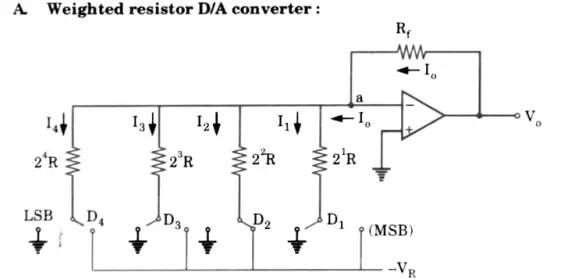
Q1.Explain working of weighted resistor D/A converter.
Answer
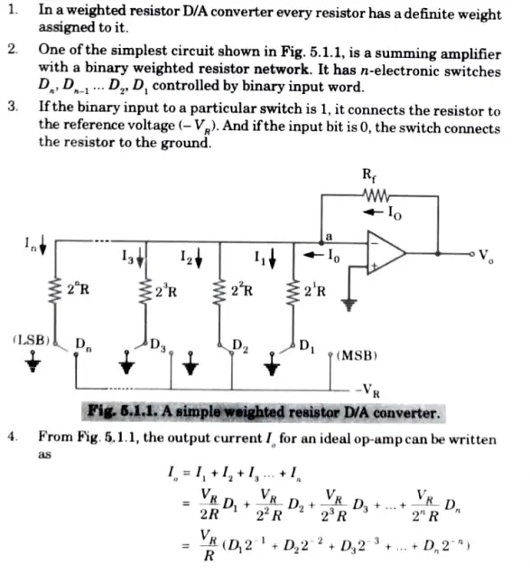
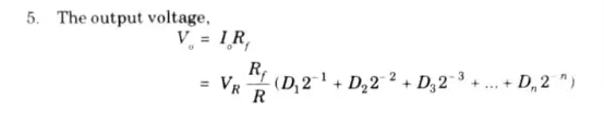
Q 2. What is a DAC ? Describe the weighted resistor DAC. Give mathematical expressions in support of your answer.
| OR |
Explain different types of DAC.
Answer
DAC: 1. It involves translating a value encoded in digital form into a voltage or current that is proportional to the digital value. A DAC or D/A converter is used to achieve this.
2. The analog voltage output V0 of an N-bit straight binary D/A converter is related to the digital input by the relation.
There are two types of D/A converters:
I. Weighted resistor D/A converter:
ii R-2R Ladder D/A converter :
1. Only the values R and 2R of resistors are used in this network. Switches under digital control are used to apply inputs to the resistor network.
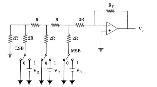
2. Consider a 3 bit R-2R Ladder D/A network. Let us assume a digital input of 001. The equivalent circuit becomes as shown in Fig. 5.3.2.
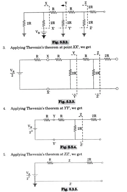
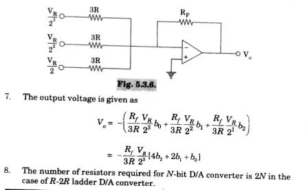
6. The equivalent resistance is 3R in each case. The circuit reduces to
Q3.Write short note on analog to digital converter (ADC).
1. The block schematic of ADC in Fig. 5.6.1 provides the function just opposite to that of a DAC.
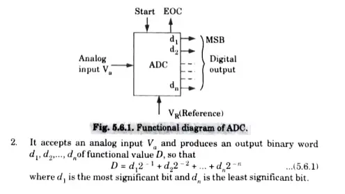
3. An ADC usually has two additional control lines, the START input to tell the ADC when to start the conversion and the EOC (end of conversion) output to announce when the conversion is complete.
4. Depending upon the type of application, ADCs are designed for microprocessor interfacing or to directly drive LCD or LED displays.
5. ADCs are classified broadly into two groups according to their conversion technique.
6. These are Direct type ADCs and Integrating type ADCs. Direct type ADCs compares a given analog signal with the internally generated equivalent signal.
7. Integrating type ADCs perform conversion in an indirect manner by first changing the analog input signal to a linear function of time or frequency and then to a digital code. The two most widely used integrating type converters are:
- Charge balancing ADC
- Dual slope ADC.
8. The most commonly used ADCs are successive approximation and the integrator type. The successive approximation ADCs are used in applications such as data loggers and instrumentation where conversion speed is important.
9. The suecessive approximation and comparator types are faster but generally less accurate than integrating type converters. The flash comparator) type is expensive for high degree of accuracy.
10. In applications where conversion accuracy is crucial, such as digital metres, panel metres, and monitoring systems, the integrated type converter is employed.
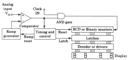
Q4. Explain the working of single slope ADC.
1. It is made up of binary counters and a ramp generator. The single slope ADC is displayed in Fig. 5.7.1.
2.At the start, the reset signal is provided to the ramp generator and the counters. Thus counters are reset to O’s.
3. The analog input voltage Vin is applied to the positive terminal of the comparator.
4.The comparator output increases since this is more positive than the negative input.
5.The comparator’s negative terminal receives the output of the ramp generator.
6.The AND gate is enabled by the comparator’s high output, which also kickstarts the ramp and allows the clock to reach the counters.
7.When the ramp voltage exceeds the input voltage, it becomes positive. The output of the comparator decreases when it exceeds V in.
8.This shuts down the AND gate, which in turn halts the counters’ timer. The latch signal needed to latch the counter data is provided by the control circuitry.
9.The ramp generator and counters are both reset by the reset signal. A decoder and a display device are then used to display the latched data.
Q 5. Explain the working of dual slope integrating ADC with the help of a circuit diagram.
- Fig. 5.8.1(a) shows the dual slop ADC functional diagram. The circuit consists of a high input impedance bufier A1. precision integrator A2 and a voltage comparator.
- The converter first integrates the analog input signal Va for a fixed duration of 2n clock periods as shown in Fig. 5.8.1(b)
- Then it integrates an internal reference voltage VR of opposite polarity until the integrator output is zero
- The number N of clock cycles required to return the integrator to zero is proportional to the value of Va averaged over the integration period. Hence, N represents the desired output code.
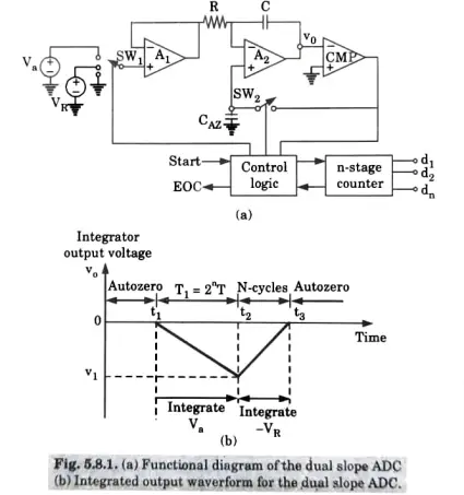
Operation
- Before the START command arrives, the switch SW1 is connected to ground and SW2 is closed.
- Any offset voltage present in the A1, A2, comparator loop after integration, appears across the capacitor CAZ till the threshold of the comparator is achieved.
- The capacitor Caz thus provides automatic compensation for the input-offset voltages of all the three amplifiers
- Later, when SW2 opens, Caz acts as a memory to hold the voltage required to keep the offset nulled.
- At the arrival of the START command at t = t1, the control logic opens SW2 and connects SW1 to Va and enables the counter starting from zero.
- The analog voltage Va is integrated for a fixed number 2n counts of clock pulses after which the counter resets to zero.
- If the clock period is T, the integration takes place for a time T1 = 2n x T and the output is a ramp going downwards as shown in Fig.5.8.1b).
- The counter resets itself to zero at the end of the interval T1 and the switch SW1 is connected to the reference voltage (-VR)
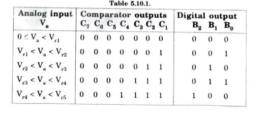
Q6. Draw and explain the flash type A/D converter. Also discuss the corresponding digital output with respect to input signal voltage.
| OR |
Design a parallel-flash ADC and explain its working.
Answer
The A/D converter most frequently used is a parallel or flash converter. Fig. depicts a 3-bit parallel comparator A/D converter.
Working
1.Let Va is the input analog voltage to be converted into digital form. The reference voltage like Vr1, Vr2 … are generated using a resistor network.
2 Va is compared simultaneously with the reference voltage by using comparators.
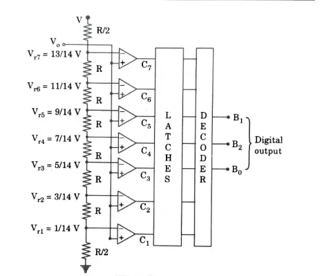
3. A decoder circuit is used to reduce a 7-bit output produced from the comparator to a 3-bit output.
4. The process adopted here is the simplest and it works quite fast.
5. With the number of bits and the accompanying complexity of the decoder circuit, the drawbacks quickly double in the number of comparators.
6. The analog input, comparator outputs and digital output are shown in Table 5.10.1]

Digital System Design Quantum, Syllabus, Important Questions
| Label | Link |
|---|---|
| Subject Syllabus | Syllabus |
| Short Questions | Short-question |
| Important Unit-1 | Unit-1 |
| Important Unit-2 | Unit-2 |
| Important Unit-3 | Unit-3 |
| Important Unit-4 | Unit-4 |
| Important Unit-5 | Unit-5 |
| Question paper – 2021-22 | 2021-22 |
Digital System Design Quantum PDF: | AKTU Quantum PDF:
| Quantum Series | Links |
| Quantum -2022-23 | 2022-23 |
AKTU Important Links | Btech Syllabus
| Link Name | Links |
|---|---|
| Btech AKTU Circulars | Links |
| Btech AKTU Syllabus | Links |
| Btech AKTU Student Dashboard | Student Dashboard |
| AKTU RESULT (One VIew) | Student Result |