
We offer the question paper with solution from the previous year. This is a 2022–23 Digital System Design Question Paper with Answer Notes. You should find this session useful for your future tests or Exams.
Dudes 🤔.. You want more useful details regarding this subject. Please keep in mind this as well.

Important Questions For Digital System Design:
*Unit-01     *Unit-02
*Unit-03    *Unit-04
*Unit-05    *Short-Q/Ans
*Question-Paper with solution 21-22
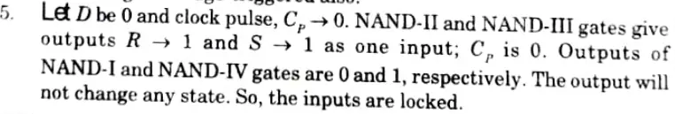
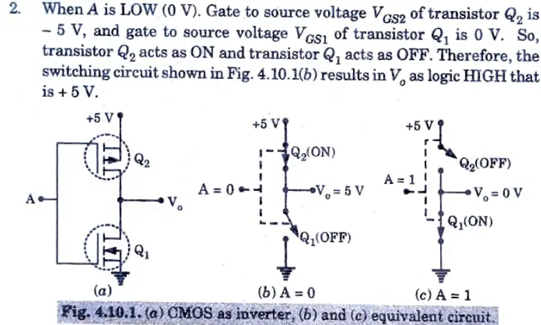
Section A – Short Question in Digital System Design Question Paper.
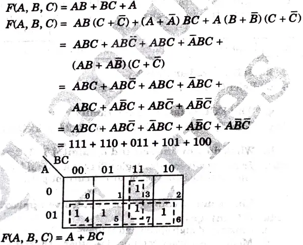
a. Simplify the expression F(A, B, C) =AB + BC+ A by K-Map.
Ans.
b. Discuss the concept of fan-in and fan-out.
Ans. Fan-out:
1. The greatest number of standard loads that a logic gate’s output may drive without compromising normal operation is known as the fan-out of the gate. The loading factor is another name for fan-out.
2. When a gate’s output is logic 1, it will spread out in the HIGH state. When a gate’s output is logic 0, it will fan out in the LOW state. The real fan-out is assumed to be the smaller of these two amounts.
3. High state fan-out is given by

Fan-in:
1. The quantity of inputs is referred to as the fan-in of a digital logic gate. An inverter, for instance, has a fan-in of 1, a NOR gate with two inputs, a NAND gate with four inputs, and so on.
2. In order to accommodate the amount of inputs, a logic designer must choose the fan-in of the gate.
3. At the hardware level, however, the fan-in provides information about the intrinsic speed of the gate itself.
4. In general, the fan-in causes a longer propagation delay. Accordingly, if both NAND gates have the same logic family, the 2-input NAND gate is faster than the 4-input NAND gate.
c. What is the role of subtractor in digital electronics ?
Ans; An electronic logic circuit known as a “subtractor” is used to compute the difference between two binary integers, the minuend and the number to be subtracted.
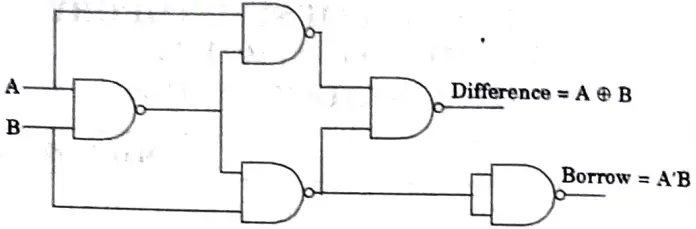
d. Construct half subtractor using NAND gates.
Ans.
e. Distinguish between shifter and barrel shifter.
Ans.
| S. No. | Shifter | Barrel shifter |
| 1. | A shifter moves bits right or left one position in one clock. | A barrel shifter is wired so you can move bits from any position to any position in a single clock. |
| 2. | It takes very few gates. | It takes a lot of gates. |
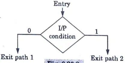
f. Define ASM and FSM.
Ans. ASM chart is composed of three basic elements : State box, decision box
and conditional box.
State box: The state of the system is indicated by a state box. The shape of the state box is a rectangle.
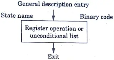
Decision box: It is a diamond shaped box used to describe the effect of an input on the control subsystem.
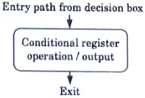
Conditional box: It is a unique box of ASM chart. The area shape of the conditional box is show a in Fig. 3.26.3. The round corners differentiate it from the state box.
g. Why is ECL the fastest logic family ?
Ans Applications requiring very high frequencies are used when the ECL family’s speed is higher. It is utilized in lightning-fast computers and extremely quick specialized applications.
h.What do you understand about digital TTL?
Ans. Bipolar transistors react to direct-current pulses in the transistor-transistor logic (TTL) digital logic circuit.
i. List some advantages of successive approximation
Ans: ‘Advantages : i. Capable of high speed and reliable.
ii. Medium accuracy compared to other ADC types.
iii. Good tradeoff between speed and cost.
j. Where is SAR ADC used?
Ans. For today’s demanding applications, high-performance, low-power ADCs can be packaged in compact form sizes thanks to the SAR design.
Section B – Important Question Notes in Digital system design
Q. Write the differences between combinational and sequential circuits.
Ans.
| S. No | Combinational circuits | Sequential circuits |
| 1. | lts output is determined by the present values of its input only. | Its output is determined by the present values of the input as well as past values of the output. |
| 2. | It does not have a memory. It does not have a feedback path from output to input. | It has a memory and a feedback path from output to input. |
| 3. | Its operation can be described by a truth table. | Its operation can be described by truth table and timing diagram. |
| 4. | It does not have a clock signal. | It may or may not have clock signal but most sequential circuit have a clock signal. |
| 5. | Its circuit is simpler than that of sequential logic circuit. | Its circuit is more complex than that ofcombinational circuits. |
| 6. | It built using basic gates i.e., NOT, AND, OR, NAND, NOR, XOR, XNOR etc. | It is built using basic gates and combinational logic circuits. |
| 7. | Eg. : Adder Subtractor, multiplexer, demux, decoder, comparator | Eg. : Flip flops, counters, shift registers. |
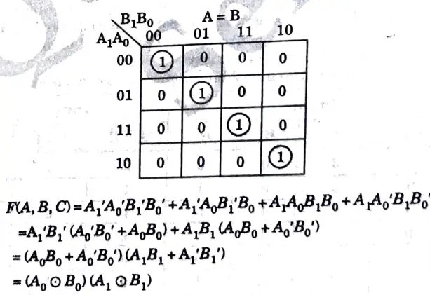
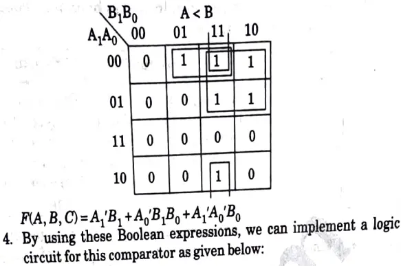
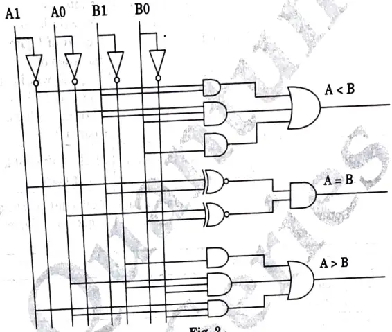
Q.Design 2-bit magnitude comparator.
Ans. A 2-bit Magnitude comparator is one that compares two binary integers with two bits each. Jt generates less tlm, equal to, and greater than between two binary values using four inputs and three outputs.·
The truth table for a 2-bit comparator is given below:
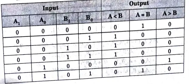
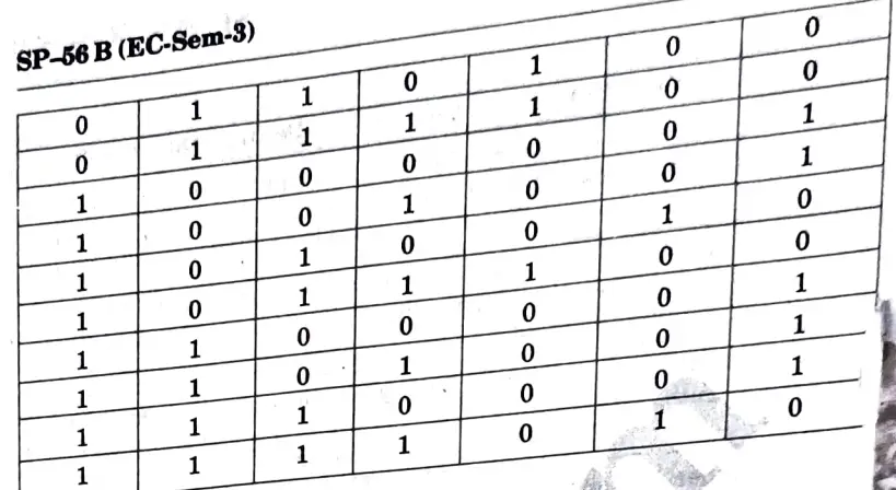
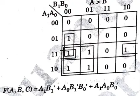
3. From the above truth table K-map for each output can be drawn a follows :
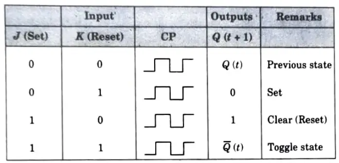
Q. Explain the working of Master-Slave JK flip-flop with the help of logic diagram, functional table, logic symbol.
Ans. 1. Master-slave combination can be constructed for any type of flip-flop by adding a gated SR flip-flop. Fig. 3.4.1 explains the master-slave operation of JK flip-flop.
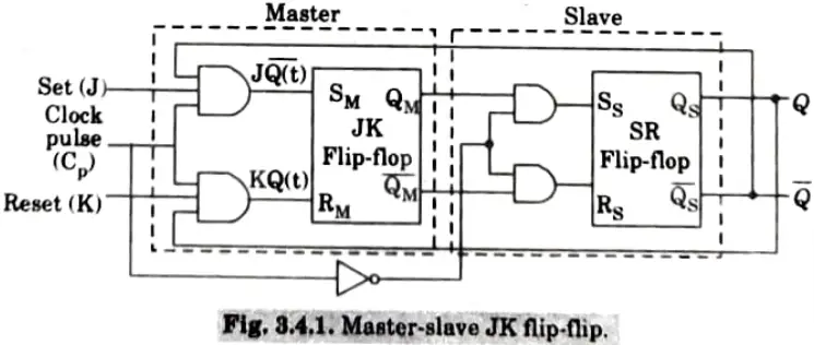
2. It requires two flip-flops where one is gated JK acts as master and other SR flip-flop acts as slave. Output of slave flip-flop is fed as input to AND gate of master flip-flop which acts as JK lip-flop.
3. Information present at JK lip-flop is transmitted to output of master flip-flop on positive level clock and is held there until negative level clock pulse appears.
4. The truth table 3.4.1 follows negative level triggering. This cascading avoids race around condition when J and K inputs are having logic-1 information.
Table – Characteristics of master and slave JK flip-flop.
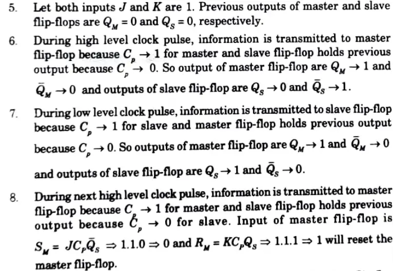
9. During low level clock pulse, information is transmitted to slave flip-flop and master flip-flop holds previous output. Slave flip-flop copies master’s output. Hence, race around situation is avoided.
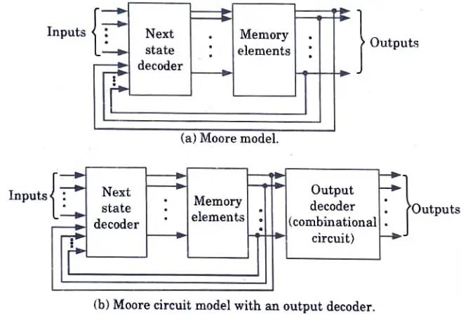
Q. i. Draw and explain block diagrams of Moore model and Mealy model.
ii. Write the difference between ripple counter and synchronous counter.
ans. i. A. Moore model:
1. When the output of the sequential network depends only on the present state of the flip-flop, the sequential network is referred to as Moore model.
2. Fig. 3.24.1 shows a sequential network which consists of two JK flip-flop and AND gates.
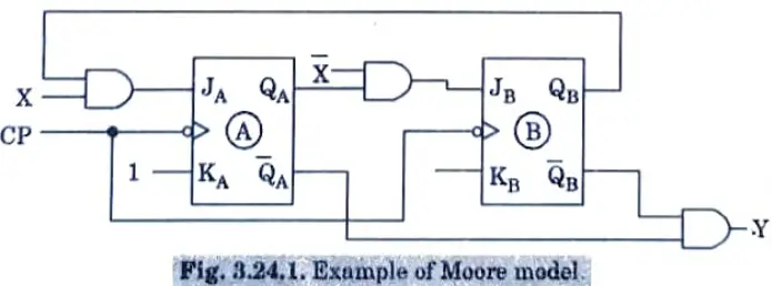
3. The network has one input X and one output Y.
4. As shown in the Fig. 3.24.2, input is used to determine the inputs of the flip-flops.
5. It is not used to determine the output.
6. The output is derived using only present states of the flip-flops or combination of it (in this case QA(bar), QB(bar)).
7. In general form the Moore model can be represented with its block schematic as shown in Fig. 3.24.2 (a) and (b).
8. In the Moore model, as output depends only on present state of the flip-flops, it appears only after the clock pulse is applied, i.e., it varies in synchronism with the clock input.
B. Mealy model:
1. When the output of the sequential network depends on both the present state of flip-flop(s) and on the inputs), the sequential circuit is referred to as Mealy model.
2. Fig. 3.25.1 shows the sample Mealy model.
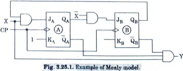
3. As shown in the Fig. 3.25.1, the output of the circuit is derived from the combination of present state of flip-flops and input(X) of the circuit.
4. Looking at Fig. 3.25.1, we can easily realize that, changes in the input within the clock pulses cannot affect the state of the flip-flop. However, they can affect the output of the circuit.
5. If the input variations are not synchronized with the clock, the derived output will also not be synchronized with the clock and we get false output (as it is synchronous sequential network).
6. The false outputs can be eliminated by allowing input to change only at the active transition of the clock (in our example HIGH-to-LOW).
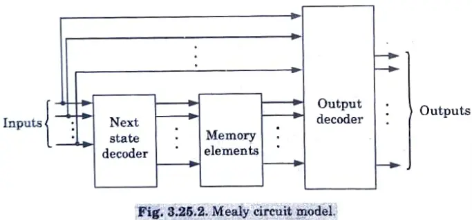
7. In general form the Mealy model can be represented with its block schematic as shown in Fig. 3.25.2.
ii. Difference between ripple (asynchronous) counter and synchronous counter :
| S. No. | Asynchronous | Synchronous | |
| 1. | Circuit | The logic circuit of this type of counters is simple to design and we feed output of one FF to clock of next FF | The circuit diagram for type of counter becomes difficult as number of states increase in the counter. |
| 2. | Propagation Time | Propagation time delay of this type of counter is: Tpd = N * (Delay of 1 FF) which is quiet high N is number of FFs | Propagation time delay of this type of counter is: Tpd = (Delay of 1 FF) + delay of 1 gate Inclusion of delay of 1 gate would be illustrated when we design higher counters: |
| 3. | Clock | Clock is same for all Flip flops | Clock is different for all Flip flops |
| 4. | Maximum operating frequency | Maximum Operating Frequency is Low | Maximum Operating frequency is Higher |
| 5. | Speed | Slow | Fast |
| 6. | Components required | Less | More |
| 7. | Cost | Less | More |
| 8. | Disadvantage | Glitches | Lock out condition |
Q. List the guidelines for construction of state graphs.
Ans. Guidelines for construction of state graphs :
- 1. Create a few sample input and output sequences first to make sure you comprehend the issue.
- 2. Identify the circumstances in which the circuit is reset.
- 3. Construct a partial state graph if only a single or a pair of sequences result in a single output.
- 4. OR determine what sequences or groups of sequences must be remembered
- 5. When adding transitions, check to see if a defined state is being transitioned to or if a new state is being added.
- 6. Make sure that there is only one transition in each state for both an O and a 1.
- 7. Add annotation or create a table to expound the meaning of each state.
Section C – digital system design previous question papers
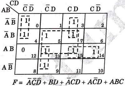
a. Minimize the following Boolean function F(A, B, C, D)= :Σm(0, 3, 4, 5, 7, 9, 13, 14, 15)
Ans.
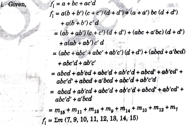
b. Expand the following into canonical form and represent in decimal form :
i. f1 =a+ be + ac’d into min terms.
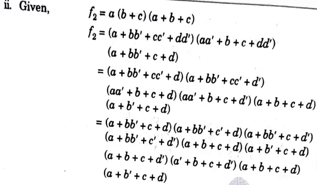
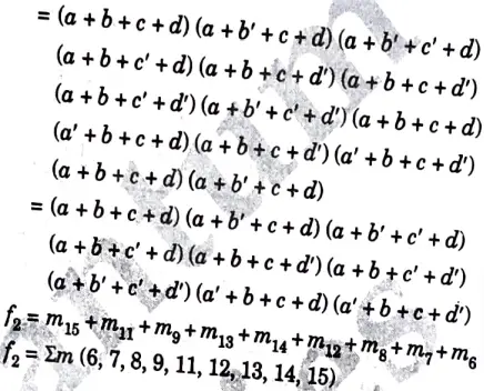
ii. f2 = a(b + c) (a+c+d) into max terms
Ans.
4. Attempt any one part of the following:
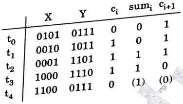
a. Explain the concept of serial adder with accumulators.
Ans.
1. The block diagram of serial adder with accumulators is shown in Fig.
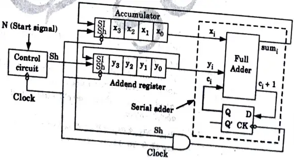
2. The full adder is used to perform bit by bit addition and D-Flip flop is used to store the carry output generated after addition.
3. This carry is used to carry input for the next addition. Initially the D Flip flop is cleared and addition starts with the least significant bits of both register.
4. After each clock pulse data within the right shift registers are shifted right 1-bit and we get from next digit and carry of precious addition as new inputs for the full adder.
5. Truth table is shown as below :
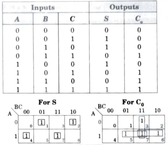
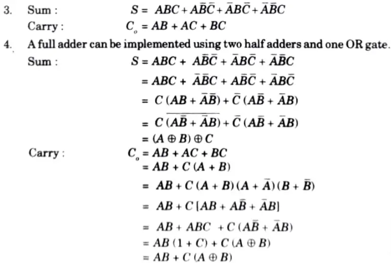
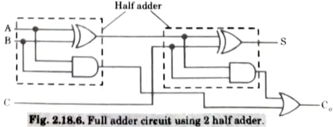
b. Design a full adder by constructing the truth table and simplifying the output equations.
Ans. Full adder:
1. Full adder is a circuit that performs the addition of three binary digits. It has three inputs A, B and C with two output S and Co where C is the previous carry. The block diagram is shown in Fig.
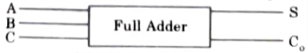
2. If there are three input variables the combinations are eight (23 = 8). Now form the truth table of the full adder.
5. Attempt any one part of the following:
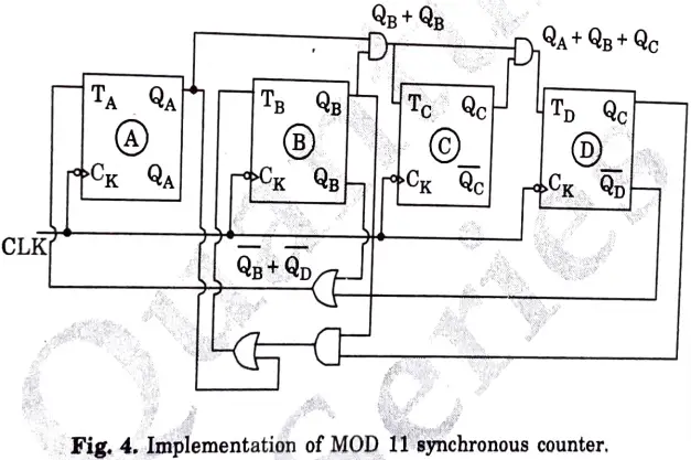
a. Design a mod 11 up ripple counter using T-FF.
Ans 1. All of the flip flops in a synchronous counter have the same clock input.
2. From 0000 to 1010, a MOD 11 synchronous counter counts. Therefore, four T flip flops are needed.
3. An excitation table is used to calculate the combinational logic of the inputs to each flip flop while designing synchronous counters.
4. The excitation table for all the four T flip flops is shown :
Table 2. Excitation table for MOD 11 synchronous counter :
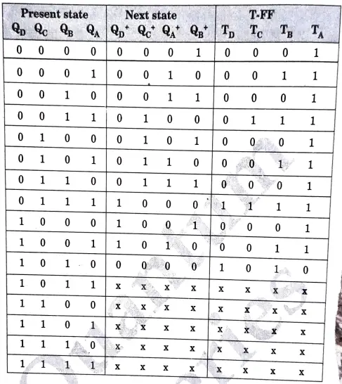
5. From the above excitation table, we can draw K-maps to determine input to every flip flop.
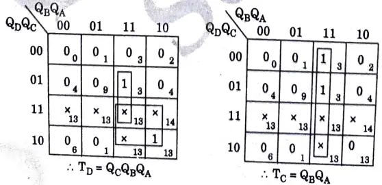
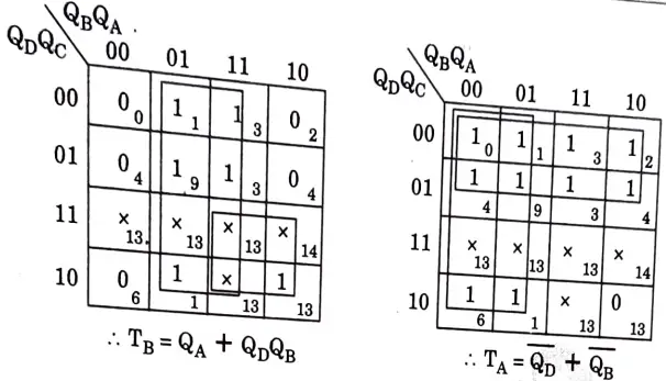
6. Four equations for four T flip flops are obtained. Using them, the MOD 11 synchronous counter is designed as follows :
b. Explain positive edge triggered D-flip-flop with the help of circuit diagram and waveforms.
Ans. 1. Edge triggered flip-flop synchronizes state change with clock pulse.
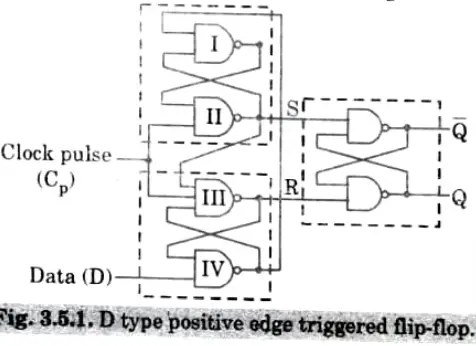
2. Output is transmitted at a specific level of clock pulse otherwise inputs are locked and flip-flop does not perform operation.
3. The operation is resumed when the clock pulse level return to zero and high level pulse occurs.
4. Flip-flop shown in Fig. 3.5.1 is positive edge-triggered flip-flop. Flip-flop can be negative edge-triggered also.
6. Attempt any one part of the following :
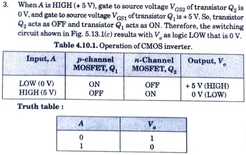
a. Draw a circuit diagram of a CMOS inverter. Draw its transfer characteristics and explain its operation.
Ans. CMOS inverter:
1. It consists of an NMOS transistor Q1 and a PMOS transistor Q2. The input is connected to the gates of both the devices and the output is at the drain of both the devices. The positive supply voltage is connected to the sources of the PMOS transistor Q2, and the source of transistor Q1 is grounded.
Characteristics of CMOS
Supply voltage: The operating range of Vpp for the 4000 and 74C series is 3 to 15 V. The VDD values for the 74HC and 74HCT series range from 2 to 6 V.
ii. Voltage levels: The output voltage levels will be very near to zero for LOW state and VDD for HIGH state when a CMOS output drives only a CMOS input and the CMOS gate has an extraordinarily high input resistance.
iii. Power dissipation: When a CMOS circuit is in a static state, its power dissipation per gate is extremely small, but it increases with increase in operating frequency and supply voltage level. For DC, CMOS power dissipation is only 2.5 nW per gate when VDD = 5 V, and it increases to 10 nW per gate when VDD = 10 V.
iv. Switching speed: “As VDD rises, the CMOS gate speed rises as well.” Power dissipation increases along with the increase in VDD.
Unused inputs: It is never recommended to leave the CMOS inputs unplugged. All CMOS inputs must be connected to either another input or a set voltage level (OV or VDD).
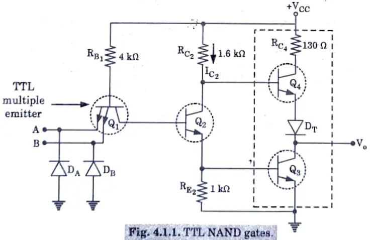
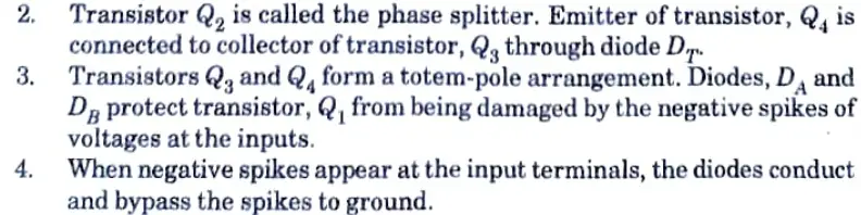
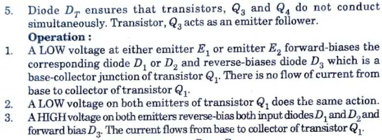
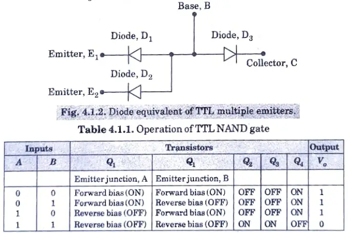
b. With the help of a neat diagram, explain the working of a two-input TTL NAND gate.
Ans. 1. The circuit of the two-input TTL NAND gate is shown in Fig. 4.1.1. The input transistor, Q1 is a multiple emitter transistor.
7. Attempt any one part of the following:
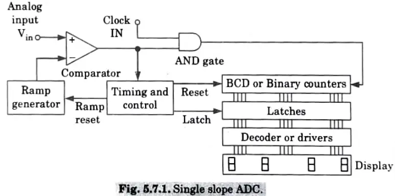
a. Explain single slope and dual slope ADC with a neat sketch.
A. Single slope ADC :
Ans.
- 1. It consists of a ramp generator and BCD or binary counters. The Fig. 5.7.1 shows the single slope ADC.
- 2. At the start, the reset signal is provided to the ramp generator and the counters. Thus counters are reset to 0’s.
- 3. The analog input voltage Vin is applied to the positive terminal of the comparator.
- 4. As this is more positive than the negative input, the comparator output goes high.
- 5. The output of ramp generator is applied to the negative terminal of the comparator.
- 6. The high output of the comparator enables the AND gate which allows clock to reach to the counters and also this high output starts the ramp.
- 7. The ramp voltage goes positive until it exceeds the input voltage. When
it exceeds Vin, comparator output goes low. - 8. This disables AND gate which in turn stops the clock to the counters. The control circuitry provides the latch signal which is used to latch the counter data.
- 9. The reset signal resets the counters to 0’s and also resets the ramp generator. The latched data is then displayed using decoder and a display device.
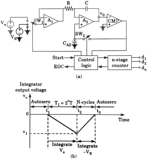
B. Dual slope ADC:
Ans.
- 1. Fig.(a) shows the dual slop ADC functional diagram. The circuit consists of a high input impedance buffer A1, precision integrator A2, and a voltage comparator.
- 2. The converter first integrates the analog input signal Va for a fixed duration of 2n clock periods as shown in Fig.(b).
- 3. Then it integrates an internal reference voltage VR of opposite polarity until the integrator output is zero.
- 4. The number N of clock cycles required to return the integrator to zero is proportional to the value of Va averaged over the integration period. Hence, N represents the desired output code.
b. Describe the switched capacitor and write its applications.
Ans. 1. Fig.5.11.1(a) shows a 4-bit switched capacitor DAC, that the capacitance values have binary weights.
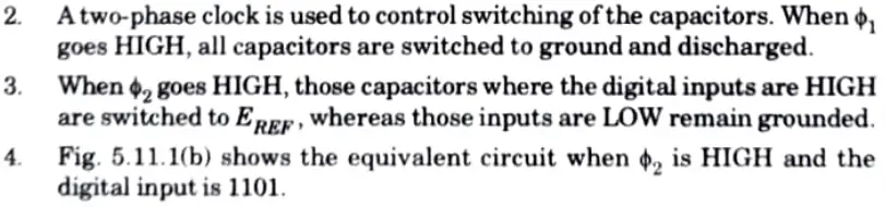
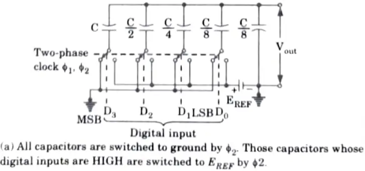
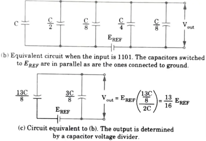
5. The capacitors whose digital inputs are 1, are in parallel and the capacitors whose digital inputs are 0, are in parallel with C/8.
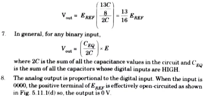
6. The circuit as shown in Fig. 5.11.1(c), where each set of the parallel capacitors is replaced by its equivalent capacitance. The output of the capacitive voltage divider is
9. For the purpose of incorporating analogue functions in integrated circuits, particularly MOS circuits, switched capacitor technology has been developed. In addition to numerous other specialized devices, it is used to build filters and amplifiers.
10. The main benefit of this technology is the ability to build tiny capacitors in integrated circuits that can replace much larger capacitors that are typically required in low-frequency analogue circuits. These capacitors are of the order of a few picofarads.

Digital System Design Quantum, Syllabus, Important Questions
| Label | Link |
|---|---|
| Subject Syllabus | Syllabus |
| Short Questions | Short-question |
| Important Unit-1 | Unit-1 |
| Important Unit-2 | Unit-2 |
| Important Unit-3 | Unit-3 |
| Important Unit-4 | Unit-4 |
| Important Unit-5 | Unit-5 |
| Question paper – 2021-22 | 2021-22 |
Digital System Design Quantum PDF: | AKTU Quantum PDF:
| Quantum Series | Links |
| Quantum -2022-23 | 2022-23 |
AKTU Important Links | Btech Syllabus
| Link Name | Links |
|---|---|
| Btech AKTU Circulars | Links |
| Btech AKTU Syllabus | Links |
| Btech AKTU Student Dashboard | Student Dashboard |
| AKTU RESULT (One VIew) | Student Result |