In this blog, We are here to explore Unit 03 Sequential Logic Design Digital System Design AKTU B.tech Important Questions. Hope this blog will help you in your upcoming exams.
Dudes 🤔.. You want more useful details regarding this subject. Please keep in mind this as well.

Important Questions For Digital System Design:
*Unit-01     *Unit-02
*Unit-03    *Unit-04
*Unit-05    *Short-Q/Ans
*Question-Paper with solution 21-22
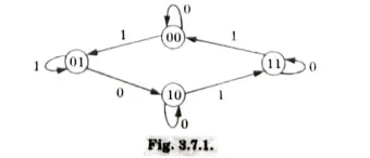
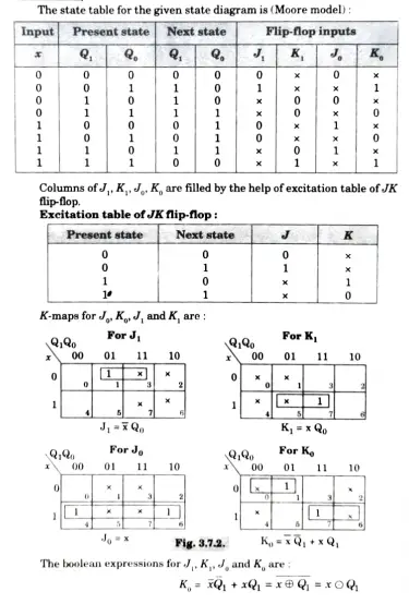
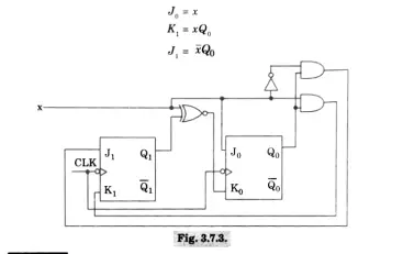
Q1. Design the clocked sequential circuit for the following state diagram using JK nip-lop.
Answer:
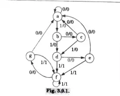
Q.2.Draw the reduced state table and reduced state diagram for the state table given in Fig. 3.9.1.
Answer
State reduction:
1. Any logic design procedure must take into account the issue of reducing the final circuit’s cost. Reducing the number of flip-flops, or states, is one method for lowering the cost.
2.Essentially, the state reduction strategy forgoes the creation of unnecessary equivalent states. Reducing redundant states lowers the need for flip-flops and logic gates, which lowers the final circuit’s cost.
3.When every possible combination of inputs results in exactly the same outputs and subsequent states, two states are said to be redundant or comparable.
4. When two states are equal, one of them can be eliminated without changing the relationship between input and output.
Numerical:
1. There are seven states, one input, and one output in the provided Fig. 3.9.1. State tables are created from the provided state diagrams.
It is evident from the state table that g and states are interchangeable. State e thus takes the role of state g.
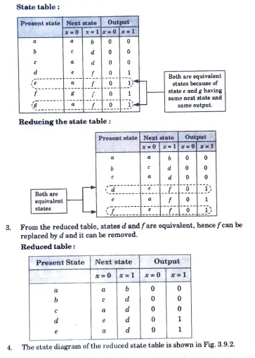
State diagram
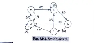
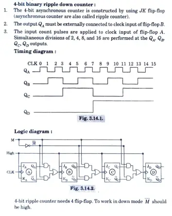
Q3. Draw diagram of a 4-bit binary ripple down counter using flip-flops that trigger on negative edge transition. Also draw a timing diagram of the counter.
| OR |
Design a ripple decade counter using JK flip-flop.
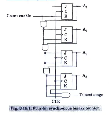
Q4. Describe the operation of a four bit synchronous binary counter with a neat sketch.
- The C inputs of all flip-flops are connected to a common clock. The counter is enabled by count enable.
- If the enable input is 0, all J and K inputs are equal to 0 and the clock does not change the state of the counter.
- The first stage A0 has its J and K equal to 1 if the counter is enabled. The other Jand Kinputs are equal to 1 ifall previous least significant stages are equal to 1 and the count is enabled.
- The chain of AND gates generates the required logic for the J and K inputs in each stage.
- The counter can be extended to any number of stages, with each stage having an additional flip-flop and an AND gate that gives an output of 1 if all previous flip-flop outputs are 1.
Q5. Write down the classification of shift registers.
| OR |
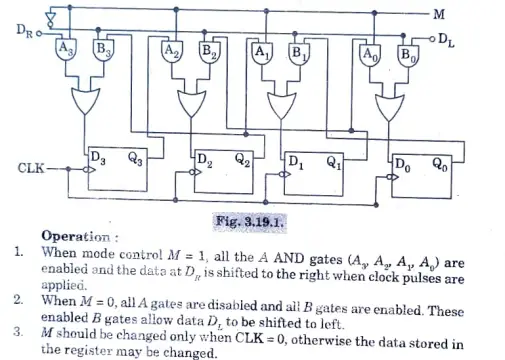
What do you mean by shift register ? What is the need of a shift register ? Draw and explain bidirectional shift register.
Answer
Shift registers:
With the use of clock pulses, binary data in a register can be transferred from one flip-flop to another inside the register or outside of it. Shift registers are the registers that permit these data transfers.
Need of register:A register is a sequential logic circuit with two basic functions:
i.Temporary storage.
ii. Shifting capability.
Classification of shift registers
Classification based on the direction of data movement:
i. Shift left register.
ii. Shift right register.
iii. Bidirectional shift registers.
2. Classification based on the mode of input and output:
i.Serial in serial out shift register (SISO)
ii. Serial in parallel out shift register (SIPO)
iii.Parallel in serial out shift register (PISO)
iv. Parallel in parallel out shift register (PIPO)
v. Universal shift register.
Bidirectional shift register:
1. It consists of four D flip-flops, four OR gates, eight AND gates and one NOT gate as shown in Fig.
Q.6.Draw and explain 4-bit universal shift register.
| OR |
Design a universal shift register that performs HOLD, SHIFT RIGHT, SHIFT LEFT, and LOAD.
Answer
1. A shift register is referred to be a universal shift register if it has the ability to load data simultaneously and shift it in both directions (shift right or shift left).
2. This shift register is capable of performing the following operations :
Parallel loading (parallel input parallel output).
i. Left shifting. ii. Right shifting.
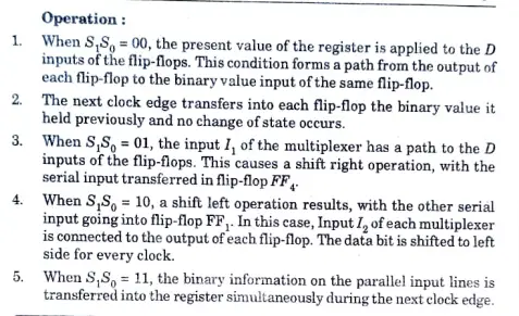
Figure 3.21.1 displays the block diagram of a 4-bit universal shift register. It is made up of 4:1 multiplexers and four D flip-flops.
4.The four multiplexers have two common select lines S1 and So. Input 10 in each multiplexer is selected when S1S0= 00, input I1 is selected when S1S0 = 01 and so on.
5. The selection inputs (S,S) control the mode of operation of the register according to the function table shown in table
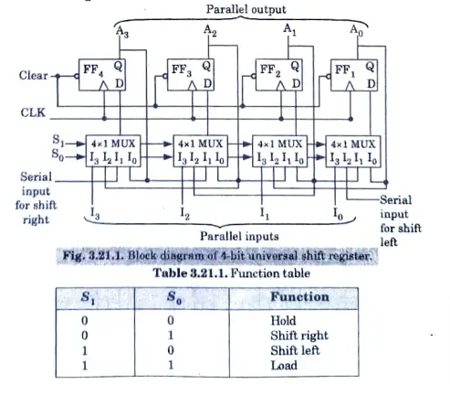
Block diagram of 4-bit universal shift register

Digital System Design Quantum, Syllabus, Important Questions
| Label | Link |
|---|---|
| Subject Syllabus | Syllabus |
| Short Questions | Short-question |
| Important Unit-1 | Unit-1 |
| Important Unit-2 | Unit-2 |
| Important Unit-3 | Unit-3 |
| Important Unit-4 | Unit-4 |
| Important Unit-5 | Unit-5 |
| Question paper – 2021-22 | 2021-22 |
Digital System Design Quantum PDF: | AKTU Quantum PDF:
| Quantum Series | Links |
| Quantum -2022-23 | 2022-23 |
AKTU Important Links | Btech Syllabus
| Link Name | Links |
|---|---|
| Btech AKTU Circulars | Links |
| Btech AKTU Syllabus | Links |
| Btech AKTU Student Dashboard | Student Dashboard |
| AKTU RESULT (One VIew) | Student Result |
3 thoughts on “Unit 03 Sequential Logic Design | Digital System Design AKTU B.tech”