
Uncover B.Tech AKTU Quantum Book Short VLSI Design Question Notes. Learn how to develop high-performance integrated circuits and advanced chip design approaches for cutting-edge technology.
Dudes 🤔.. You want more useful details regarding this subject. Please keep in mind this as well.

Important Questions For VLSI Design:
*Quantum               *B.tech-Syllabus
*Circulars                *B.tech AKTU RESULT
* Btech 4th Year    * Aktu Solved Question Paper
Unit-I: Introduction VLSI Design (Short Question)
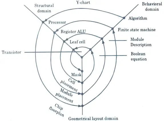
Q1. Draw Y-chart.
Ans. The Y-chart consists of three domains of representation namely behavioral, structural and geometrical layout domain.
Q2. What are the advantages of VLSI design process ?
Ans. Advantages of VLSI design process :
- 1. Reduced size for circuits.
- 2. Increased cost-effectiveness for devices.
- 3. Improved performance in terms of the operating speed of circuits.
- 4. Requires less power than discrete components.
- 5. Higher device reliability.
- 6. Requires less space and promotes miniaturization.
Q3. Define critical path.
Ans. The critical path is defined as the path with the greatest delay between an input and an output. Once the circuit timing has been determined, the crucial path can be easily identified using the traceback method.
Q4. What do you mean by high integration density ?
Ans. A high integration density means a large number of components in a small area.
Q5. Define VLSI.
Ans. When the number of active devices per chip exceeds hundreds of thousands, it is referred to as very large scale integration (VLSI). Almost all current chips use the VLSI approach.
Q6. State Moore’s law in reference to VLSI design.
Ans. It states that the number of transistors on a microchip increases every two years, while computer prices are cut in half.
Q7. Write down the applications of FPGA.
Ans. The applications of FPGA are:
- 1. Digital signal processing
- 2. Bio-informatics
- 3. ASIC prototyping
- 4. Medical imaging
Q8. What is the classification of IC packages ?
Ans. The classification of IC packages is as follows:
- 1. Dual In-line Packages (DIP)
- 2. Pin Grid Array (PGA) Packages
- 3. Chip Carrier Packages (CCP)
- 4. Quad Flat Packs (QFP)
- 5. Multi-Chip Modules (MCM).
Q9. What do you mean by regularity ?
Ans. Regularity implies that the hierarchical breakdown of a big system should provide as many simple and related blocks as possible.
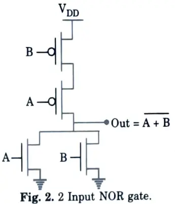
Q10. Give the circuit arrangement for 2 input NOR gate using CMOS logic.
Ans.
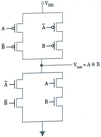
Q11. Implement Ex-OR gate using CMOS logic.
Ans.
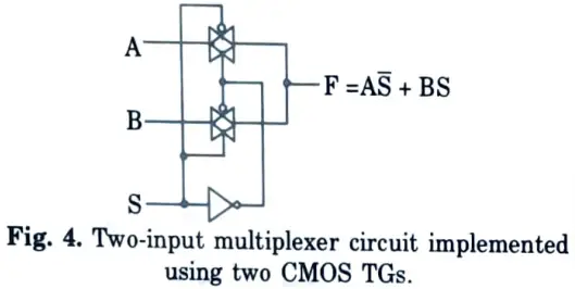
Q12. Implement 2:1 MUX using CMOS transmission gate.
Ans.
Q13. Why we prefer CMOS transmission gates over other gates?
Ans. 1. Complex gates can be constructed with a small number of transistors, reducing parasitic.
2. By combining pMOS and nMOS in a transmission gate design, the problem of reduced noise margin, higher switching resistance, and increased static power dissipation is avoided.
Unit-II: Interconnect Parameters (Short Question)
Q1. Define the term Interconnect.
Ans. The wires linking transistors together are called interconnect.
Q2. Define the term interconnect impact in brief.
Ans. Interconnect impact examines the delay, energy, and noise impact of cables that electrically connect two or more circuit parts.
Q3. Define the term interconnect delay.
Ans. While signal propagation via wires limits state-of-the-art circuit speed, interconnection delay is the fundamental performance metric for wires.
Q4. What do you mean by lumped RC model ?
Ans. A basic approach combines the total wire resistance of each wire segment into a single R and the capacitance into a single C. The lumped RC model is a simple model.
Q5. Define RC delay model.
Ans. The RC delay model approximates a switching transistor with an effective resistance and allows for delay estimation via arithmetic rather than differential equations.
Q6. Estimate tpd for a unit inverter driving m identical unit inverters.
Ans.1. Fig. shows an equivalent circuit for the falling transition.
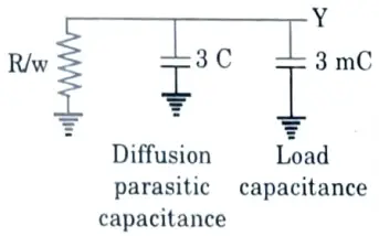
- 2. Since, each load inverter presents 3C units of gate capacitance, therefore total gate capacitance = 3 mC
- 3. Parasitic capacitance at output node = 3C
- 4. The resistance is R, so the Elmore delay, tpd = (3 + 3m) RC
Q7. Define logical effort with example.
Ans. The logical effort of a gate is defined as the ratio of the gate’s input capacitance to the input capacitance of an inverter capable of delivering the same output current.
Q8. What is parasitic delay ?
Ans. A gate’s parasitic delay is the time it takes to drive zero load. It is possible to estimate it using RC delay models.
Q9. Define the fanout of the gate.
Ans. The fanout of the gate, h, is the ratio of the load capacitance to the input capacitance.
Q10. What is Miller effect ?
Ans. If the inverter is biased in its linear region near VDD/2, the Cgd is multiplied by the large gain of the inverter. This is known as the Miller effect.
Q11. What do you mean by scaling ? Also write its techniques.
Ans.
- 1. Scaling of MOS transistors is concerned with the gradual reduction of overall device dimensions as permitted by available technology while keeping the geometric ratios present in larger devices.
- 2. There are two basic types of size-reduction techniques :
- i. Full scaling (also called constant-field scaling) and
- ii. Constant-voltage scaling.
Unit-III: Dynamic CMOS Design (Short Question)
Q1. Write the properties of dynamic circuit.
Ans.
- 1. Dynamic logic has higher speed than equivalent static family.
- 2. It occupies less area.
- 3. It is non-ratioed.
- 4. Dynamic logic always require clock.
Q2. Bring out the drawbacks of dynamic logic.
Ans. Drawbacks of dynamic logic are :
- 1. Always require clocks.
- 2. Design is more difficult.
Q3. Mention the advantages of dynamic logic circuits over static logic circuits.
Ans. In general, dynamic logic implementation of complex functions requires less silicon area than static logic implementation.
Q4. Write the classification of high performance dynamic CMOS circuits.
Ans. 1. Domino CMOS circuits.
2. NORA CMOS circuits.
3. Zipper CMOS circuits.
Q5. Write short notes on zipper CMOS circuits.
Ans. With the exception of the clock signals, the basic circuit architecture of zipper CMOS is basically identical to that of NORA CMOS. The zipper CMOS clock signal architecture necessitates the development of somewhat different clock signals for precharge and pull-down transistors.
Q6. Write the disadvantages of NORA CMOS logic circuit. How can be eliminated it.
Ans. Charge sharing and leakage are also issues with NORA CMOS. A circuit approach known as Zipper CMOS can be utilised to overcome dynamic charge sharing and soft node leakage.
Q7. What are the advantages of NORA CMOS logic circuit ?
Ans. Advantages of NORA CMOS logic circuit are:
- 1. Static CMOS inverter is not required at the output of every dynamic logic state.
- 2. Compatible with domino CMOS logic.
- 3. It allows pipelined system architecture.
Q8. Enlist the properties of domino logic gates.
Ans. Properties of domino logic gates are:
- 1. Each gate requires N + 4 transistors.
- 2. Logic evaluation propagates as falling Dominoes hence minimum evaluation period is determined by the logic depth.
- 3. Inputs must be stable (only one rising transition) during the evaluation period.
- 4. Gates are ratioless and non-inverting.
Q9. What are the different types of sequential CMOS circuit?
Ans. Sequential CMOS circuit can be classified into three main groups :
- i. Bistable
- ii. Monostable
- iii. Astable
Q10. What do you mean by bistable circuit ?
Ans. Bistable circuits contain two table states or operation modes that can be achieved given specific input and output conditions.
Q11. Draw the diagram of SR latch based on NOR gates.
Ans.
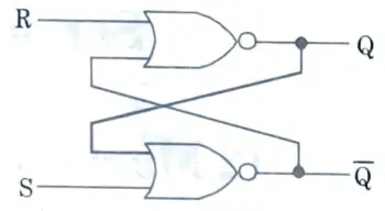
Q12. What are the disadvantage of SR latch ?
Ans. The disadvantage of an SR latch is that when both S and R are high, its output state becomes indeterminant.
Unit-IV: Semiconductor Memories (Short Question)
Q1. How many types of semiconductor memory ?
Ans. There are two types of semiconductor memory
- i. RAM (Random Access Memory)
- ii. ROM (Read Only Memory).
Q2. What is ROM ?
Ans. ROMs are non-volatile memories, which means that the recorded data is not lost even when the power is turned off, and no refresh operation is necessary.
Q3. What do you understand by dynamic RAM cell ?
Ans. The DRAM cell is made up of a capacitor that stores binary information ‘1’ (high voltage) or ‘0’ (low voltage) and a transistor that allows the capacitor to be accessed. DRAM is commonly utilised for main memory because of its low cost and great density.
Q4. Define SRAM cell.
Ans. When the SRAM cell is made up of a latch, the cell data is retained as long as the power is turned on, and no refresh operation is required, as with DRAM cells. SRAM is primarily employed in cache memory in a variety of applications.
Q5. Distinguish between SRAM and DRAM.
Ans.
| S. No. | DRAM | SRAM |
| 1. | The DRAM cell consists of a capacitor to store binary information. | SRAM cell consists of a latch to store the binary information. |
| 2. | DRAM is high density and low cost memory. | SRAM is mainly used for the cache memory applications. |
Q6. Enlist the advantages of using address multiplexing scheme in DRAM cell.
Ans. Advantage of using address multiplexing scheme in DRAM cell are:
- 1. It reduces the chip package size by reducing pin count.
- 2. Reduction of packaging cost.
Q7. What do you understand by flash memory ?
Ans. The flash memory cell is made up of a single transistor with a floating gate, the threshold voltage of which can be changed repeatedly by applying an electrical field to its gate.
Q8. How the limitations of a ROM based realization is overcome in a PLA-based realization ?
Ans. The encoder section of a ROM is solely programmable, and using ROMs to realise boolean operations is often wasteful because there is no cross-connect for a major chunk. This waste can be avoided by employing a Programmable Logic Array (PLA), which takes up substantially less chip space.
Q9. What do you mean by latch-up ? What is the latch-up problem ?
Ans. A. Latch-up: Latch-up is described as the formation of a low-impedance link between the power supply rails and the ground rails in CMOS chips as a result of the connectivity of parasitic pnp-npn bipolar transistors.
B. Latch-up problem: These BJTs generate an SCR with positive feedback and effectively short circuit the power rail to ground, resulting in high current flow and perhaps irreversible device damage.
Q10. How the latch-up problem can be overcome ?
Ans. 1. Reduce the gains of BJT by lowering the minority carrier lifetime through gold doping of the substrate.
2. Use minimum area p-wells, so that the p-well photocurrent can be minimized during transient pulses.
Q11. Why leakage power dissipation has become an important issue in deep submicron technology ?
Ans. Leakage and subthreshold currents are the most significant sources of leakage power dissipation in deep submicron technology. As a result, leaky power dissipation has emerged as a critical issue in deep submicron technology.
Q12. Why we need a low power VLSI circuits in today’s scenario ?
OR
What are needs for low power VLSI chips ?
Ans. Because we need
- i. Extended battery life.
- ii. Low cost.
- iii. High reliability.
Q13. What are the factors that reduces the power dissipation ?
Ans.
- 1. Reduction of power supply voltage VDD.
- 2. Reduction of the voltage swing at all nodes.
- 3. Reduction of the load capacitance.
- 4. Reduction of switching probability.
Q14. Comment on overview of power consumption in CMOS logic circuits.
Ans. The average power Consumption in conventional CMOS digital circuits can be expressed as the sum of three main components, namely :
- i. The dynamic (Switching) power consumption
- ii. The short-circuit power consumption and
- iii. The leakage power consumption
Q15. Why short-circuit power dissipation occurs ?
Ans. Short-circuit power dissipation happens when both pMOS and nMOS transistors in the circuit conduct concurrently during the switching time. They form a direct current path between the power supply and ground at this moment.
Q16. What is the effect on power consumption if the parasitic capacitance is reduced ?
Ans. The goal of reduction of parasitic capacitance is low power consumption.
Q17. Write the levels of design for which switching capacitance can be reduced.
Ans.1. System level design.
2. Circuit level design.
3. Physical level design.
Unit-V: Introduction to Testing (Short Question)
Q1. Write the types of defects in designing of digital circuits.
Ans. The types of defects in designing of digital circuits are :
- 1. Physical defects.
- 2. Electrical defects.
- 3. Logical defects.
Q2. Define the terms:
Defects, Errors and Faults.
Ans. Defect: A defect in an electronic system is an inadvertent divergence between the hardware that has been implemented and the planned design.
Fault: A representation of a “defect” at the abstracted function level is called a fault.
Error: A wrong output signal produced by a defective system is called an error.
Q3. What are the difficulties for the test engineer to test the VLSI circuits?
Ans. 1. The complexity of VLSI systems.
2. With minor exceptions, there is no way that the circuit can be modified during test to make it work.
Q4. What is the major difficulty in sequential circuit testing ?
Ans. The major difficulty in sequential circuit testing is to determine the internal state of the circuit.
Q5. Explain the terms controllability and observability.
Ans. A. Controllability: A circuit’s controllability is a measure of how easily (or how difficultly) the controller can establish a specified signal value at each node by setting values at the circuit input terminals.
B. Observability: The observability is a measure of the ease (or difficulty) with which each logic node in the circuit may be determined by managing its primary input and monitoring its primary output.
Q6. What is use of BST (Boundary Scan Test) ?
Ans. This technique uses scan route and self testing to tackle challenges related with testing VLSI circuits on boards.
Q7. What are the advantages of BST test ?
Ans. Advantages of BST are as follows :
- 1. No need for complex factors.
- 2. The test engineer’s work is simplified.
- 3. Fault coverage is increased.
Q8. Write the objectives of Built-In-Self-Test.
Ans. The objectives of Built-In-Self-Test are :
- 1. To reduce test pattern generation cost.
- 2. To reduce the volume of test data.
- 3. To reduce test time.
Q9. Write the expression of dynamic power dissipation for MOS circuit.
Ans. The dynamic power dissipation may be represented as :
Pdynamic = α CVDD2f
Q10. Differentiate between static power and dynamic power.
Ans.
| S. No. | Static power | Dynamic power |
| 1. | Static power is the circuit leakage power. | The power used to charge or discharge the intrinsic capacitor of a transistor is referred to as dynamic power. |
| 2. | Static power exists even if there are no activities. | Dynamic power only exists when signals toggle either from low-to-high or high-to-low. |
Q11. Write the modules which are essential circuit modules for BIST.
Ans. 1. Pseudo random pattern generator (PRPG).
2. Output response analyzer (ORA).
Q12. What are the fabrication defects which can be detected by IDDQ test only ?
Ans.
- 1. Gate oxide short.
- 2. p-n diode leakage.
- 3. Transmission-gate defects.
- 4. Channel punch-through.
Q13. Write the design guidelines for IDDQ testability.
Ans.
- 1. Full CMOS is preferred.
- 2. No active pull-ups or pull-downs.
- 3. No internal drive conflicts.
- 4. No floating nodes in the circuits.
Q14. Write the physical defects (faults) that can occur in CMOS.
Ans. 1. Defects in Si substrates.
2. Photolithographic defects.
3. Oxide defects.
Q15. What are the electrical faults that can be translated into logical faults ?
Ans. 1. Logical stuck-at-0 or stuck-at-1.
2. Slower transition (delay fault).
3. AND-bridging, OR-bridging.
Q16. What is meant by stuck-at-1 (s-a-1) fault and stuck-at-0 (s-a-0) faults.
Ans. 1. Faults are fixed (0 or 1) value to a net which is an input or an output of a logic gate or a flip-flop in the circuit.
2. If the net is stuck to 0, it is called stuck-at-0 (s-a-0) fault.
3. And if the net is stuck to 1, it is called stuck-at-1 (s-a-1) fault.

VLSI Design Btech Quantum PDF, Syllabus, Important Questions
| Label | Link |
|---|---|
| Subject Syllabus | Syllabus |
| Short Questions | Short-question |
| Question paper – 2021-22 | 2021-22 |
VLSI Design Quantum PDF | AKTU Quantum PDF:
| Quantum Series | Links |
| Quantum -2022-23 | 2022-23 |
AKTU Important Links | Btech Syllabus
| Link Name | Links |
|---|---|
| Btech AKTU Circulars | Links |
| Btech AKTU Syllabus | Links |
| Btech AKTU Student Dashboard | Student Dashboard |
| AKTU RESULT (One View) | Student Result |