
VLSI Design: The previous year’s question paper with answers for B.Tech AKTU contains a significant number of exam-oriented questions and extensive explanations that will assist you in preparing for VLSI design examinations.
Dudes 🤔.. You want more useful details regarding this subject. Please keep in mind this as well.

Important Questions For VLSI Design:
*Quantum          *B.tech-Syllabus
*Circulars           *B.tech AKTU RESULT
* Btech 4th Year
Section A: Short Question In VLSI Design
a. What is Photolithography ?
Ans. Photolithography is a microfabrication process for patterning parts on a thin film or the bulk of a substrate.
b. Why we need a low power VLSI circuits in today’s scenario ?
Ans. Because we need :
- i. Extended battery life.
- ii. Low cost.
- iii. High reliability.
c. What is contamination delay ?
Ans. The contamination delay is the shortest amount of time that the outputs retain a previous value after the inputs change.
d. Define logical effect with example.
Ans. The logical effort of a gate is defined as the ratio of the gate’s input capacitance to the input capacitance of an inverter capable of delivering the same output current.
e. Differentiate between static power and dynamic power.
Ans.
| S. No. | Static power | Dynamic power |
| 1. | Static power is the circuit leakage power. | Dynamic power is the power used to charge or discharge transistor intrinsic capacitor. |
| 2. | Static power exists even if there are no activities. | Dynamic power only exists when signals toggle either from low-to high or high-to-low. |
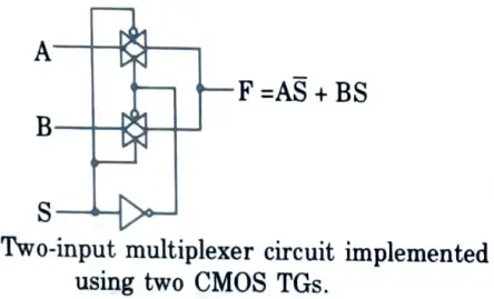
f. Implement 2 : 1 MUX using CMOS transmission gate.
Ans.
g. Describe different storage elements.
Ans.
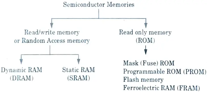
h. Distinguish between SRAM and DRAM.
Ans.
| S. No. | DRAM | SRAM |
| 1. | The DRAM cell consists of a capacitor to store binary information. | SRAM cell consists of a latch to store the binary information. |
| 2. | DRAM is high density and low cost memory. | SRAM is mainly used for the cache memory applications. |
i. Explain the term controllability and observability.
Ans.
- A. Controllability: A circuit’s controllability is a measure of how easily (or how difficultly) the controller can establish a specific signal value at each node by setting values at the circuit input terminals.
- B. Observability: The observability is a measure of the ease (or difficulty) with which any logic node in the circuit can be determined by controlling its primary input and observing its primary output.
j. What is meant by Stuck-at-1 fault and Stuck-at-0 fault ?
Ans.
- 1. Faults are fixed (0 or 1) value to a net which is an input or an output of a logic gate or a flip-flop in the circuit.
- 2. If the net is stuck to 0, it is called stuck-at-0 (s-a-0) fault.
- 3. And if the net is stuck to 1, it is called stuck-at-1 (s-a-1) fault.
Section B : Long Questions of VLSI Design
a. Discuss the hierarchy of various semiconductors with Moore’s law. Write short note on VLSI testing.
Ans. A. Hierarchy of various semiconductors with Moore’s law :
- 1. Jack Kilby of Texas Instruments invented the integrated circuit in February 1959. In July 1959, Robert Noyce at Fairchild developed the planar version of the IC. Since then, this technology’s evolution has been extremely rapid.
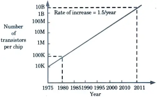
- 2. One way to assess the field’s progress is to examine the complexity of ICs as a function of time.
- 3. When we plot the log of the component count as a function of time, we get a straight line, indicating that chip complexity has grown exponentially over the last three decades.
- 4. As Gordon Moore noted early on, the component count has roughly doubled every 18 months. Moore’s law refers to this regular doubling.
- 5. The ability to shrink or scale devices is the primary factor that has enabled this increase in complexity.
- 6. Clearly, smaller ICs can pack a greater number of components with greater functionality, which is also advantageous in terms of faster ICs that consume less power.
- 7. Fig. shows the level of integration versus time for memory chips.
- 8. It can be seen that logic chips contain significantly fewer transistors in any given year, owing to the large consumption of chip area for complex interconnects.
- 9. Because memory circuits are highly regular, more cells can be integrated with much less interconnect space.
- 10. Demand for digital CMOS ICs will remain strong due to distinguishing features such as low power, reliable performance, and high-speed circuit techniques such as dynamic circuits.
- 11. It is now predicted that the minimum feature size in CMOS integrated circuits will drop to 35 nm within a decade.
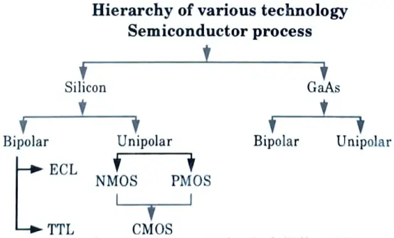
- 12. For very high speed circuits, bipolar and gallium arsenide (GaAs) circuits have been used, and this practise may continue. MMIC and GaAs MESFET technology have been extremely successful.
- 13. As long as CMOS technology continues to scale down, other technologies are likely to be the technology of tomorrow.
b. Explain Elmore delay model with suitable RC networks. Mention its merits.
Ans. A. Lumped RC model: A first approach combines the total wire resistance of each wire segment into a single R and the capacitance into a single C. The lumped RC model is a simple model.
B. Register capacitor network (Elmore delay model) :
1. Consider the resistor-capacitor network of Fig.
2. The result of this circuit topology is that there exists a unique resistive path between the source node s and any node i of the network. The total resistance along this path is called the path resistance Rii.
3. For example, the path resistance between the source node s and node 4 is,
R44 = R1 +R3 +R4
4. The shared path resistance Rik, which represents the resistance shared among the paths from the root node s to nodes k and i:
Rik = Ri (Ri [path(s i).. path(s k)])
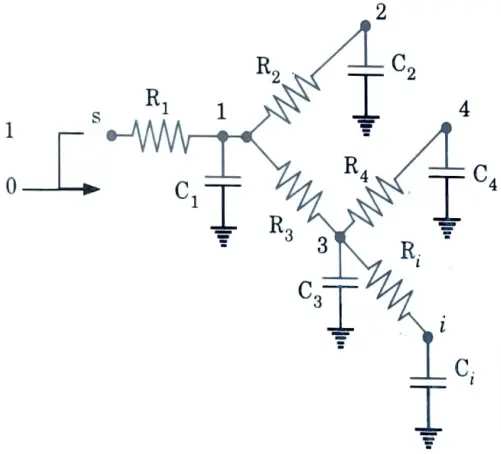
5. Assume now that each of the N nodes of the network is initially discharged to GND, and that a step input is applied at node s at time t = 0.
6. The Elmore delay at node i is then given by the following expression :
C. Merits of Elmore delay model :
- i. Simple closed-form expression.
- ii. Useful for interconnect optimization.
- iii. Upper bound of 50 % delay.
- iv. High fidelity.
c. Compare the performance of Domino CMOS logic and NP Domino CMOS logic with suitable example.
Ans.
| S. No. | Domino CMOS | NP Domino CMOS |
| 1. | Domino CMOS circuit has inverter at the output of each stage, so it requires more transistors. | Since NP Domino circuit has no inverter at the output of each stage, it is generally composed of fewer transistors. |
| 2. | It provides only non-inverting signals at the output. | It provides both inverting and non-inverting signals at the output. |
| 3. | Domino CMOS circuit had challenges like instability and charge-sharing. | NP Domino CMOS are immune to the problems of instability and charge-sharing. |
| 4. | Low area utilization in Domino CMOS. | High area utilization in NP Domino CMOS. |
| 5. | Power dissipation is high in Domino CMOS. | Power dissipation is low in NP Domino CMOS. |
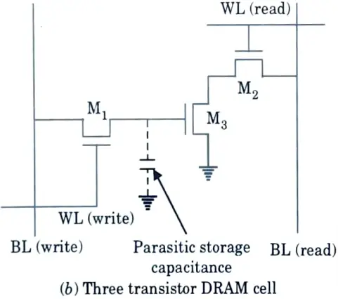
d. Explain read/write operation of SRAM memory cell. How 1 bit cell is used in bigger memory systems.
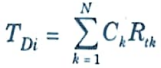
Ans. A. Read/write operation of SPAM memory cell :
- 1. Assume Q is initially 0 and thus Ǭ is initially 1. Ǭ and bit line C bar (C–) both should remain 1.
- 2. When the word line is raised, bit line C should be pull down through driver and access transistors M1 and M3.
- 3. At the same time C is being pull down, node Q tends to rise. Qis held low by M1, but raised by current flowing in from M3. Hence, the driver M1 must be stronger than the access transistor M3.
- 4. Specifically, the transistor must be ratioed such that node Q remains below the switching threshold of the M6/M2 inverter. This constraint is called read stability.
- 5. Waveforms for the read operation are shown in Fig. as 0 is read onto C.
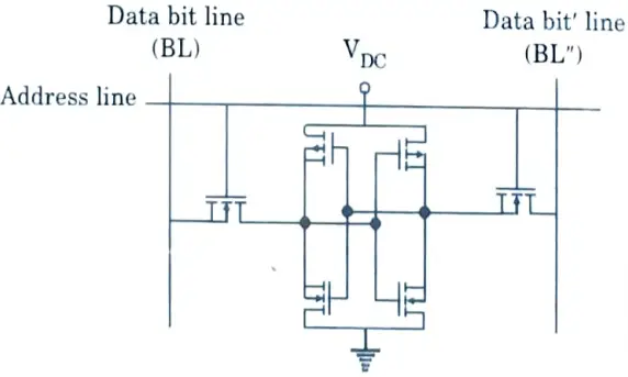
B. 1-bit cell :
- 1. A SRAM chip is made from an array of cells, where each cell can store one bit information. A cell is made from flip-flop.
- 2. The flip-flops consist of six (or four) transistors. The basic block of a SRAM cell is shown in Fig.
- 3. Since these devices require only power supply to retain the data, they are also referred as static memory.
- 4. Address line is used to select the cell while the data bit is written to (or read from) the cell using a data bit line.
- 5. A large number of such cells are arranged in matrix form to get biggest storage capacity.
- 6. The 61xx family of memory chips is SRAM, where xx in the chip number represent capacity in kbits, for example, 6116 has 16 kbits (organized as 2k x 8) bits.
e. Explain the issues involved in BIST techniques in details.
Ans. A. Scan based techniques :
- 1. Scan design techniques are a structured approach to designing sequential circuits that incorporates testability from the start.
- 2. The most difficult aspect of sequential circuit testing is determining the circuit’s internal state.
- 3. Scan design techniques aim to improve internal state controllability and observability.
B. Built in self-test techniques :
- 1. As the complexity of individual VLSI circuits and overall system complexity rises, test generation and application become an expensive and inefficient means of testing.
- 2. In addition, the high speed at which many VLSI systems are designed to operate creates extremely difficult problems.
- 3. Such issues necessitated the use of highly sophisticated, but not always affordable, test equipment.
- 4. The objectives of this test are:
- i. To reduce test pattern generation cost.
- ii. To reduce the volume of test data.
- iii. To reduce test time.
Compact Test :
- 1. Data compression techniques are currently used in BIST systems, and they consist of comparing system test responses rather than the entire test data, which can be enormous in some cases.
- 2. The test compacting scheme used most is called signature analysis. Here the data is represented as a polynomial P(r) which is divided by a characteristic polynomial C(x) to give the signature R(x), so that
R(x) = P(x)/ C(x)
This analysis is represented in Fig.
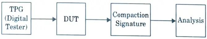
- 3. The DUT’s (Device Under Test) signature is compared to the expected signature to determine if the DUT is fault-free.
- 4. The difference between the faulty and good signatures can also be used to determine the nature of the fault.
- 5. Another data compression technique known as transition counting has been in use for quite some time.
- 6. It involves counting transitions in a specific direction (0 to 1 or 1 to 0) and comparing this count to the count obtained from the simulation model.
Section 3 : VLSI Design Process
a. Draw the Y-chart and explain VLSI design process. Mention its advantages.
Ans. A. Y-chart :
- 1. The chart was first introduced by D. Gajski. Y-chart illustrates a simplified design flow for most logic chips, using design activities on three different domains which resemble the letter Y.
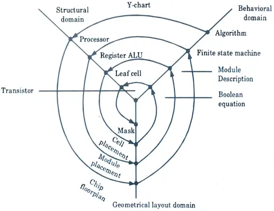
- 2. The Y-chart consists of three domains of representation namely behavioral, structural and geometrical layout domain.
- 3. The design flow starts from algorithm that describes the behavior of the target chip.
- 4. The corresponding architecture of the processor is then defined. It is mapped onto the chip surface by floor-planning as shown in Fig.
- 5. The following design evolution defines FSM implementation using registers and ALU. CAD tools are then used to place these modules geometrically on the chip surface.
- 6. The third evolution begins with the description of a behavioural module. Leaf cells are then used to implement individual modules. A cell placement and routing programme can be used to place logic gates (leaf cells).
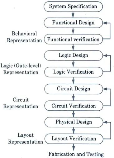
- 7. The final stage entails the generation of leaves and masks. The diagram below depicts a more simplified view of the VLSI design flow.
- 8. Keep in mind that design verification is critical at every stage of this process.
- 9. The failure of design during verification causes expensive re-design at latter stage and results in increased time to market.
- 10. Although top-down design flow appeals for design process, but in reality there is no uni-directional top-down design flow. Both top-down and bottom-up approaches have to be combined for a successful design.
B. Advantages :
- 1. Reduced size for circuits.
- 2. Increased cost-effectiveness for devices.
- 3. Improved performance in terms of the operating speed of circuits.
- 4. Requires less power than discrete components.
- 5. Higher device reliability.
- 6. Requires less space and promotes miniaturization.
b. Explain the CMOS fabrication steps with neat diagram using n-well process.
Ans. MOS IC fabrication technique:
- 1. The fabrication process involved a set of patterned layers of doped silicon, polysilicon, metal and insulating silicon dioxide.
- 2. Initially silicon substrate has to be taken as shown in Fig. 1(a).
- 3. The sequence starts with the thermal oxidation of the silicon surface, results in growth of about 1 mm thickness of SiO2 layer as shown in Fig. 1(b).
- 4. The entire layer is coated with the substance called photoresist., which is a light sensitive, acid-resist organic polymer as shewn in Fig. 1(c).
- 5. When photoresist material is exposed to UV light the exposed portion become soft so that solvents can easily etch that portion.
- 6. To select the specified position for exposure we use mask, it allows the passage of UV light from its transparent portion as shown in Fig. 1(d).
- 7. The type of photoresist initially hard in nature but when exposed to light becomes soft are known as positive photoresist.
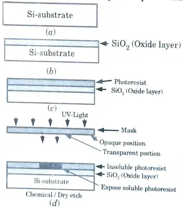
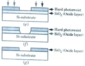
- 8. Following the UV exposure step, the soft portion is etched off using solvents (HF acid) as shown in Fig. 1(e).
- 9. Now, the SiO2 region which is not covered can be etched away by using chemical solvents shown in Fig. 1(f).
- 10. We obtain an oxide window that reaches down to the silicon surface, the remaining photoresist can now be stripped from rest of SiO2 surface by using another solvents as shown in Fig. 1(g).
- 11. The sequence of fabrication step actually is a single pattern transfer on to the SiO2 surface.12. The fabrication of semi-conductor devices requires several such pattern transfer to be performed on SiO2, polysilicon and metal.
Section 4 : RC Delay Model
a. Derive the expression for total power dissipation of a CMOS circuit.
Ans. A. Sources of power dissipation :
1. Power dissipation in CMOS circuits comes from two components :
- A. Dynamic dissipation due to :
- a. Charging and discharging load capacitances as gates switch.
- b. “Short-circuit” current while both pMOS and nMOS stacks are partially ON.
- B. Static dissipation due to:
- a. Subthreshold leakage through OFF transistors.
- b. Gate leakage through gate dielectric.
- c. Junction leakage from source/drain diffusions.
- d. Contention current in ratioed circuits.
Putting this together gives the total power of a circuit
Pdynamic = Pswitching +Pshort circuit
Pstatic = (Isub + Igate + Ijunct + Icontention)VDD
Ptotal = Pdynamic + Pstatic
- 2. Power can also be considered in active, standby and sleep modes.
- 3. Active power is the power consumed while the chip is doing useful work. It is usually dominated by Pswitching.
- 4. Standby power is the power consumed by the chip while it is idle. When clocks are stopped and ratioed circuits are disabled, leakage determines the standby power.
- 5. In sleep mode, unneeded circuit supplies are turned off to prevent leakage. This drastically reduces the amount of sleep power required, but because the chip requires time and energy to wake up, sleeping is only possible if the chip is idle for a long enough period of time.
B. Static power consumption :
- 1. Considering the static CMOS inverter shown in Fig., if the input = ‘0’, the associated nMOS transistor is OFF and the pMOS transistor is ON. The output voltage is VDD of logic ‘1’.
- 2. When the input = ‘1′, the associated nMOS transistor is ON and the pMOS transistor is OFF. The output voltage is 0 volts (GND).
- 3. Keep in mind that when the gate is in either of these logic states, one of the transistors is always turned off. When the circuit is quiescent, that is, when no transistors are switching, no current flows through the OFF transistor, so power dissipation is zero.
- 4. The primary advantage of CMOS over competing transistor technologies is zero quiescent power dissipation. Secondary effects such as subthreshold conduction, tunnelling, and leakage, on the other hand, cause small amounts of static current to flow through the OFF transistor.
- 5. Assuming that the leakage current is constant and that the instantaneous and average power are equal, static power dissipation is the product of total leakage current and supply voltage.
Pstatic = Istatic VDD
B. Dynamic power consumption :
- 1. The primary dynamic dissipation component is charging the load capacitance. Suppose a load Cis switched between GND and VDD at an average frequency of fsw.
- 2. Over any given interval of time T, the load will be charged and discharged Tfsw times. Current flows from VDD to the load to charge it. Current then flows from the load to GND during discharge.
- 3. In one complete charge/discharge cycle, a total charge of = CVDD is thus transferred from VDD to GND.
- 4. The average dynamic power dissipation is
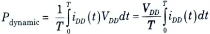
Taking the integral of the current over some interval T as the total charge delivered during that time, we simplify to
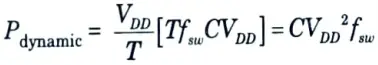
- 5. Because most gates do not switch every clock cycle, it is often more convenient to express switching frequency fsw as an activity factor 𝞪 times the clock frequency f. Now, the dynamic power dissipation may be rewritten as:
Pdynamic = 𝞪 CVDD2f
b. Draw and explain the working of RC delay model for interconnects.
Ans. RC delay models approximate the non-linear transistor I-V and C-V characteristics with an average resistance and capacitance over the switching range of the gate.
- A. Effective resistance :
- 1. The RC delay model treats a transistor as a switch in series with a resistor. The effective resistance is the ratio of Vds to Ids averaged across the switching interval of interest.
- 2. A unit nMOS transistor is defined to have effective resistance R.
- 3. An nMOS transistor of K times unit width has resistance R/K because it delivers K times as much current.
4. A unit pMOS transistor has greater resistance, generally in the range of 2R-3R, because of its lower mobility. - 5. According to the long-channel model, current decreases linearly with channel length and hence resistance is proportional to L.
- 6. Moreover, the resistance of two transistors in series is the sum of the resistances of each transistor.
7. However, if a transistor is fully velocity-saturated, current and resistance become independent of channel length. - 8. The resistance of transistors in series is somewhat lower than the sum of the resistances, because series transistors have smaller V, and are less velocity-saturated.
- 9. The effect is more pronounced for nMOS transistors than pMOS because of the higher mobility and greater degree of velocity saturation.
- B. Gate and diffusion capacitance :
- 1. Each transistor has gate and diffusion capacitance.
- 2. A transistor of k times unit width has capacitance kC.
- 3. Diffusion capacitance depends on the size of the source/drain region. Wider transistors have proportionally greater diffusion capacitance.
- 4. Increasing channel length increases gate capacitance proportionally but does not affect diffusion capacitance.
Section 5 : NORA and TSPC Dynamic CMOS Logic
a. Draw and explain NORA and TSPC dynamic CMOS logic.
Ans. A. NORA :
- 1. This design alternative to domino CMOS logic eliminates the output buffer without causing clock and data race problems that occur when cascading dynamic gates.
- 2. NORA CMOS (No-Race CMOS) eliminates race issues by cascading alternate nMOS and pMOS blocks for logic evaluation. Routing two complemented clock signals costs money.
- 3. The cascaded NORA gate structure is shown in Fig.
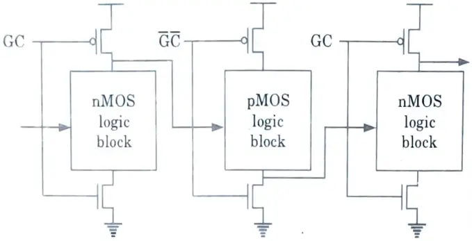
- 4. When the global clock (GC) is low (G bar C bar (G–C–)high), the nMOS logic block output nodes are precharged high, while outputs of gates with pMOS logic blocks are pre charged low. When the clock changes, gates are in the evaluate state.
B. TSPC (True Single Phase Clock) dynamic CMOS logic :
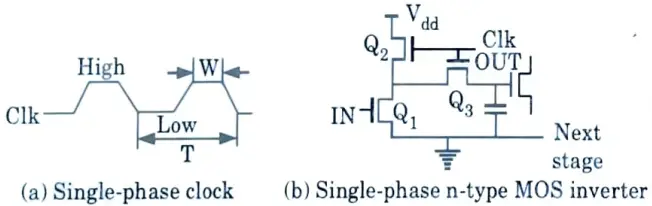
- 1. Single-phase clock consists of a sequence of pulses having high and low levels with width W and time period T as shown in Fig.(a).
- 2. A single-phase clock has two states (low and high) and two edges per period.
- 3. The schematic diagram of a single-phase dynamic nMOS inverter is shown in Fig.(b).
- 4. When the clock is in the high state, both transistors Q2 and Q3 are ON. Depending on the input, Q1 is either ON or OFF.
- 5. If the input voltage is low, Q1 is OFF and the output capacitor charges to VDD through Q2 and Q3.
- 6. When the input voltage is high, Q1 is ON and the output is discharged through it to a low level.
- 7. When the clock is in the low state, the transistors Q2 andQ3 are OFF, isolating the output capacitor. This voltage is maintained during the OFF period of the clock, provided the period is not too long.
- 8. During the period, the power supply is also disconnected and no current flow through the circuit. As current flows only when the clock is high, the power consumption is small, and it depends on the duty cycle.
- 9. It may be noted that the output of the circuit is also ratioed, because the low output voltage depends on the ratio of the ON resistance of Q1 to that of Q2 (ratio of high time to the time period T). 10. As we know that, this ratio is related to the physical dimensions of Q1 to Q2 (Low ratio) and is often referred to as the inverter ratio.
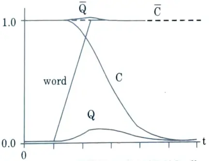
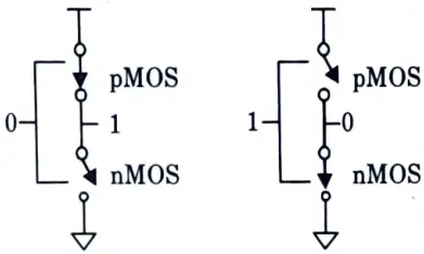
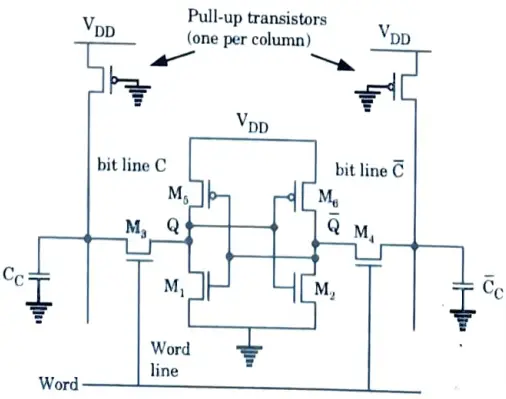
b. What is pre-charge evaluate logic in dynamic CMOS logic and draw the basic architecture of SRAM and DRAM.
Ans. A. Pre-charge evaluate logic in dynamic CMOS logic :
- a. Precharge :
- i. When CLK = 0, the output node, Out is precharged to VDD by the pMOS transistor Mp. During that time, the evaluate nMOS transistor Me is OFF, so that the pull-down path is disabled.
- ii. The assessment FET eliminates static power consumption during the precharge period (this is, static current would flow between the supplies if both the pull down and the precharge device were turned ON simultaneously ).
- b. Evaluation :
- i. For CLK = 1, the precharge transistor Mp is OFF, and the evaluation transistor Me is turned ON.
- ii. The output is conditionally discharged based on the input values and the pull-down topology.
- iii. If the inputs are such that the PDN conducts, then a low resistance path exists between Out and GND and the output is discharged to GND.
- B. Architecture of SRAM : The circuit diagram of SRAM cell is shown in Fig.
C. Architecture of DRAM :
Section 6 : DRAM Cell
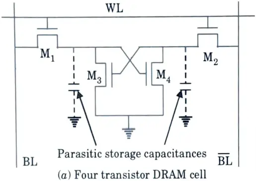
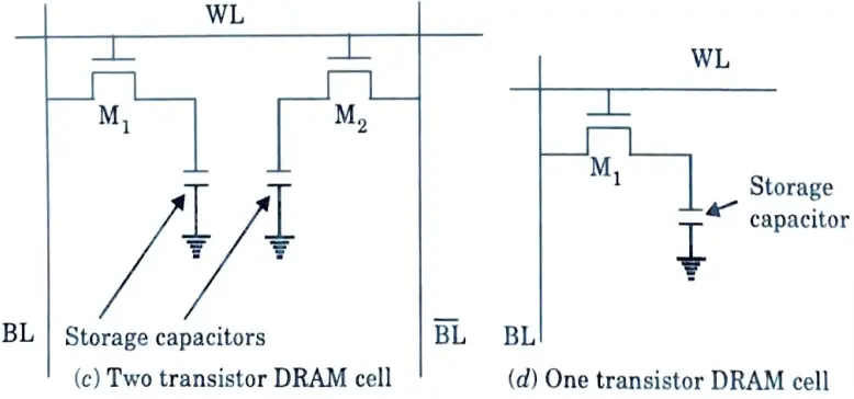
a. Write short note on DRAM cell. Explain leakage and refresh operation in DRAM cells.
Ans. A. DRAM : The DRAM cell consists of a capacitor to store binary information ‘1’ (high voltage) or ‘0’ (low voltage) and a transistor to access the capacitor. Due to low cost and high density DRAM is widely used for main memory.
B. Leakage and refresh operation :
1. Different leakage mechanisms contribute to the decay of charge at the cell and total leakage current is expressed as
Ileakage = Isub + Itunneling + Ij + Icell-to-cell
where Isub is the leakage current through the cell access transistor, Itunneling is the tunneling current through thin dielectric material, Ij is the junction leakage current at the storage node,
Icell-to-cell is the leakage current across the field oxide.
2. As the minimum feature size is scaled-down Ij tends to take a smaller portion of the total leakage current and Icell-to-cell is usually negligible due to the thick field oxide as in the trench isolation technique.
3. Since Isub is a strong function of the threshold voltage, increasing VSB of the access transistor is an effective and practical method to reduce this leakage component.
4. The refresh operation to recharge the cell capacitor is accomplished by reading and restoring operations for the cell using different control signals than those used for the normal read/write operations.
5. A feature of all refresh operations is that the DRAM chip does not send the cell data out to the external devices.
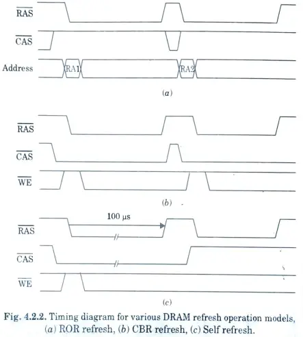
6. Fig. shows typical timing diagrams for refresh operations called ROR (RAS bar (RAS–) – only refresh), CBR(CAS bar (CAS–) – before – RAS bar (RAS–)) refresh and self refresh.
b. Explain the various types of power dissipation in CMOS circuits.
Ans. A. Sources of power dissipation :
1. Power dissipation in CMOS circuits comes from two components :
- A. Dynamic dissipation due to :
- a. Charging and discharging load capacitances as gates switch.
- b. “Short-circuit” current while both pMOS and nMOS stacks are partially ON.
- B. Static dissipation due to:
- a. Subthreshold leakage through OFF transistors.
- b. Gate leakage through gate dielectric.
- c. Junction leakage from source/drain diffusions.
- d. Contention current in ratioed circuits.
Putting this together gives the total power of a circuit
Pdynamic = Pswitching +Pshort circuit
Pstatic = (Isub + Igate + Ijunct + Icontention)VDD
Ptotal = Pdynamic + Pstatic
- 2. Power can also be considered in active, standby and sleep modes.
- 3. Active power is the power consumed while the chip is doing useful work. It is usually dominated by Pswitching.
- 4. Standby power is the power consumed by the chip while it is idle. When clocks are stopped and ratioed circuits are disabled, leakage determines the standby power.
- 5. In sleep mode, unneeded circuit supplies are turned off to prevent leakage. This drastically reduces the amount of sleep power required, but because the chip requires time and energy to wake up, sleeping is only possible if the chip is idle for a long enough period of time.
Section 7 : Parallel Processing Approach
a. Explain the parallel procession approach in low power CMOS circuits.
Ans. Parallel processing approach :
- 1. Another method for sacrificing area in exchange for low power dissipation is to employ parallelism or hardware replication. Consider N identical processing elements, each with function F (INPUT), as shown in Fig.
- 2. The consecutive input vectors arrive at the same rate as in the single stage case and are routed to all of the N processing blocks’ registers.
- 3. Gated clock signals, with period NTCLK are used to load each register every N clock cycles.
- 4. Each input register is clocked at lower frequency of fCLK/N, the time allowed to compute the function for each input vector is increased by factor of N.
- 5. This implies that the VDD can be reduced until the critical path delay equals the new clock period of NTCLK.
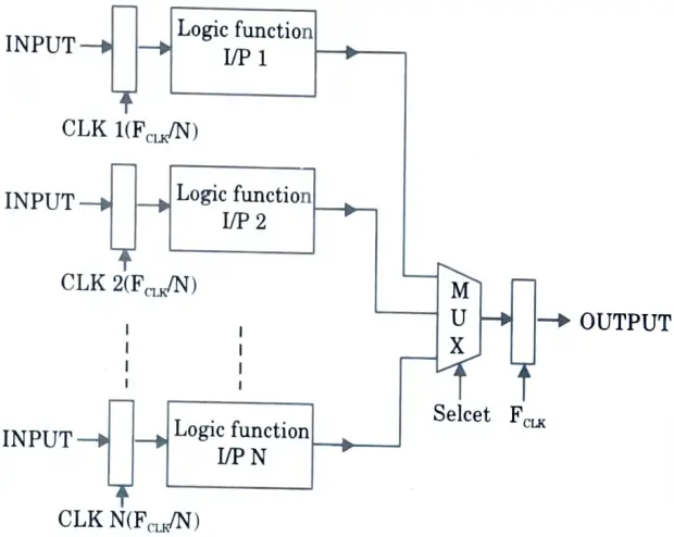
- 6. The output of the N processing blocks are multiplexed and send to output register ensuring the same data throughput rate as before.
- 7. The timing diagram of this parallel arrangement is shown in Fig.
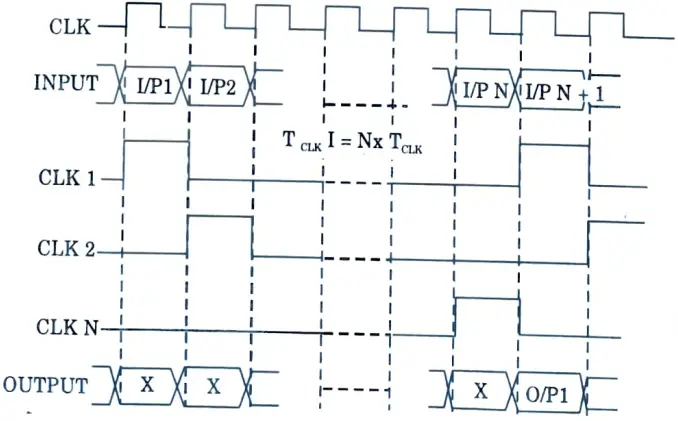
- 8. The total dynamic power dissipation of the parallel structure is found as the sum of the power dissipated by the input registers and logic blocks at clock frequency of fCLK/N, and output register operating at clock frequency of fCLK.
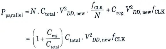
- 9. The amount of power reduction achievable in N-block parallel implementation is
- 10. Two consequences of this approach are increased area and the increased latency.
- 11. A total of N identical processing blocks must be used to slow down the operating speed by a factor of N.
- 12. Actually the silicon area will grow even faster than the number of processors because of signal routing and overhead circuitry.
b. Write a short note on :
i. Scan cell based approach.
Ans. i. Scan cell based approach :
- 1. Scan design techniques are a structured approach to designing sequential circuits that incorporates testability from the start.
- 2. The most difficult aspect of sequential circuit testing is determining the circuit’s internal state.
- 3. Scan design techniques aim to improve internal state controllability and observability.
- The scan path:
- 1. The sequential circuit for scan path is shown in Fig.
- 2. Scan path design techniques modify the logic so that the inputs and outputs of the combinational part can be accessed and the storage element reconfigured to form the scan path.
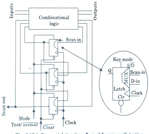
- 3. The storage elements are usually LD, JK, or RS flip-flop elements with the classical structure being modified by the addition of a two way multiplexer on the data input.
- 4. In figure a basic D flip-flop has been shown with the added input multiplexer. This configuration is commonly known as MD’ (multiplexed D) flip-flop.
- 5. The sequential circuit containing the scan path has two modes of operation a normal and a test mode.
- 6. The configuration associated with each basic mode is set out in Fig.(a) and Fig.(b) normal and test mode respectively.
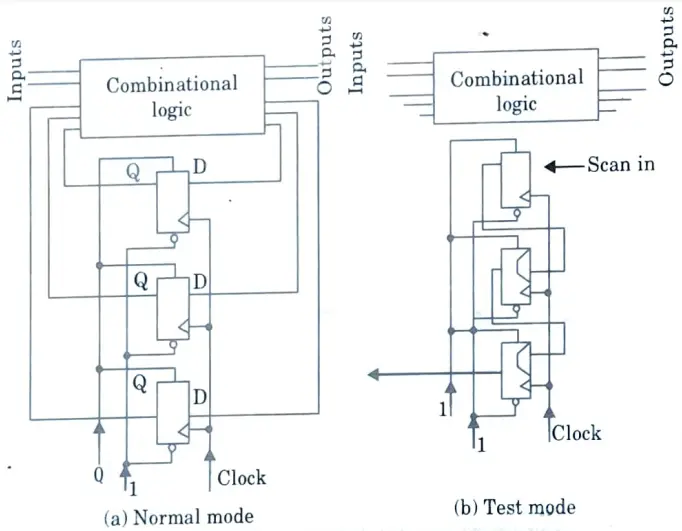
- 7. Before applying test patterns, the scan path shift register is verified by shifting in all ones then all zeros.
- 8. A general method for testing with the scan path approach is as follows:
- i. Set the mode to test so that the scan path is configured.
- ii. Verify the scan path by shifting test data in and out.
- iii. Set the shift register to a known initial state.
- iv. Apply a test pattern to the primary inputs of the overall circuit.
- v. Set the mode to normal. The circuit then settles and the primary outputs are monitored.
- vi. Activate the circuit with one clock pulse.
- vii. Return to the test mode.
- viii. Scan out the contents of the scan path registers and simultaneously scan in next pattern.
- ix. Repeat from step (iv) etc.
2 thoughts on “VLSI Design: Last year Question Paper Questions with Answer Btech AKTU”