Learn about Integrated Circuits B.Tech AKTU Quantum Book Short Question Notes. Learn the fundamentals of creating intricate electronic circuits on a single chip for a variety of applications.
Dudes 🤔.. You want more useful details regarding this subject. Please keep in mind this as well.

Imporant Questions For Integrated Circuits:
*Quantum               *B.tech-Syllabus
*Circulars                *B.tech AKTU RESULT
* Btech 3rd Year    * Aktu Solved Question Paper
Unit-I: The 741 IC Op-Amp (Short Question)
Q1. What is the function of the output stage or last stage of Op-Amp?
Ans. The function of the last stage i.e., the output stage of an Op-Amp is to supply the load current and provide a low impedance output. it should also provide a large output voltage saving ideally the total supply voltage i.e., VCC + VEE.
Q2. Define and give significance of slew rate.
Ans. Slew rate: Slew rate is defined as the maximum rate of change of output voltage with time. Its unit is V/μsec.
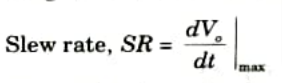
Significance: The output voltage of an ideal Op-Amp may instantaneously follow changes in the input step voltage because the slew rate of an ideal Op-Amp is unlimited. The performance of Op-Amp improves as slew rate increases.
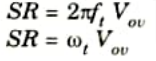
Q3. Give the relationship between ft and SR.
Ans. The relationship is given by
Q4. What do you mean by DC analysis of a circuit ?
Ans. 1. DC operating point analysis determines how a circuit will behave under the influence of a DC voltage or current.
2. The bias point, also known as the quiescent point, Q-point, is the general name for the analysis’s output.
3. The outcomes of the DC Operating point analysis are often intermediate values for more in-depth study.
Q5. What is CMRR ? Give its mathematical term.
Ans. The relative sensitivity of an Op-Amp to a difference signal as compared to a common mode signal called common mode rejection ratio (CMRR) and gives the figure of merit ρ for the differential amplifier. So, CMRR is given by
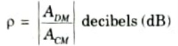
where ADM is differential mode gain and ACM is common mode gain.
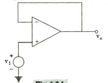
Q6. Define voltage follower.
Ans. In the non-inverting amplifier of Fig. if Rf = 0 and R1 = . Then the output voltage is equal to the input voltage both in magnitude and phase. Hence, the circuit is called a voltage follower.
Q7. Write advantage of a voltage follower circuit.
Ans. 1. Low output impedance, almost zero.
2. The output follows the input exactly without a phase shift.
Q8. Why the bias circuit is used ?
Ans. The bias circuit is used to provide proportional current in the collector of transistor.
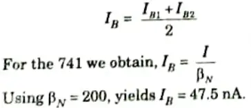
Q9. Define input bias current.
Ans. The input bias current of an Op-Amp is defined as,
Q10. What is the role of coupling capacitor (Cc) in 1C-741 internal circuit ?
Ans. The role of coupling capacitor (Cc) in IC. 741 internal circuit is to compensate frequency using the Miller compensation techniques. Coupling capacitor (Cc) is connected at the stage-I feedback path.
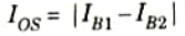
Q11. What is input offset current and input offset voltage?
Ans. A. Input offset current: The input offset current is defined as,
B. Input offset voltage: In the 741 Op-Amp, the input offset voltage is due to mismatches between Q1 and Q2 between Q3 and Q4 between Q5 and Q6 and between R1 and R2.
Q12. Why ideal Op-Amp draw no current at both the input terminals ?
Ans. An ideal Op-Amp draws no current at both the input terminals i.e., i1 = i2 = 0 because of infinite input impedance any signal source can drive it and there is no loading on the preceding driver stage.
Q13. How the effect of input bias current in non-inverting amplifier is compensated?
Ans. The effect of input bias current in a non-inverting amplifier is compensated by placing a compensating resistor Rcomp in series with the input signal V1.
Q14. State the reasons for the offset currents at the input of the Op-Amp.
Ans. 1. The base currents of the two transistors employed in the input stage serve as the op-input amp’s currents. Preferably, two currents should be equal and these transistors should be properly matched.
2. Nevertheless, because to a mismatch between two transistors, the two input base currents really deviate somewhat from one another. Input offset current is the phrase used to describe the difference in currents flowing into the Op-two Amp’s input terminals.
Unit-II: Linear Applications of IC Op-Amps (Short Question)
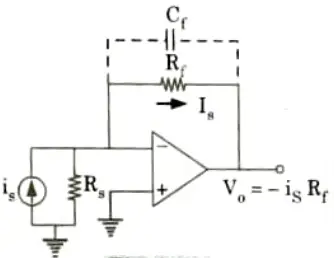
Q1. Draw the circuit diagram of current to voltage converter (transresistance amplifier).
Ans.
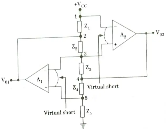
Q2. Draw and explain the generalized impedance converter circuit.
Ans. 1. Generalized impedance converters (GIC) are Op-Amp circuits that employ RC networks for simulating frequency-dependent impedance elements such as inductors. Fig. shows the circuit of: a GIC.
2. The input impedance of the circuit
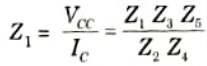
3. Eq. shows that the circuit shown in Fig. 2.1.1, can be used as grounded impedance whose nature and value depends on the nature and values of impedance elements Z1 to Z5.
Q3. What are the requirements of power amplifier?
Ans. i. For maximum power transfer, it should have a low output impedance to enable impedance matching.
ii. High efficiency of electricity conversion.
iii. Heat sinks must be employed since a significant quantity of power is lost at the power transistor junction.
Q4. Write the use of an instrumentation amplifier.
Ans. When measuring physical quantities like temperature, water flow, etc., a transducer is used to sense low level signals that can be amplified by an instrumentation amplifier.
Q5. What are the important features of an instrumentation amplifier?
Ans. i. High gain accuracy.
ii. High CMRR.
iii. High gain stability with low temperature coefficient.
Q6. Write the advantages of active filters.
Ans.
- i. No loading problem.
- ii. Flexibility in gain and frequency adjustment.
- iii. Low cost.
- iv. Small component size.
Q7. What are the limitations of active filters over passive filters?
Ans. 1. The active filter is now designed for high frequencies.
2. Unlike filters, active expensive filters need a dual-polarity DC power source. passive
3. The active element is susceptible to changes in process parameters and is sensitive to environmental factors like temperature.
Q8. Write the advantage of active filter over passive filter.
Ans. 1. Easier to tune or adjust.
2. Active filter is small and less bulky.
Q9. Differentiate wide band and narrow band pass filter.
Ans.
| S. No. | Wide band pass filter | Narrow band pass filter |
| 1. | The wide band pass filter uses two Op-Amp. | The narrow band pass filter uses one Op-Amp. |
| 2. | It has one feedback path. | It has two feedback path. |
| 3. | The Op-Amp in the non-inverting configuration. | The Op-Amp in the inverting configuration. |
Q10. What do you mean by a frequency response of a filter circuit ?
Ans. 1. Frequency response, which is used to describe the dynamic of the system, is a quantitative measurement of the output spectrum of a filter circuit in reaction to a stimulus.
2. It is a comparison of the output’s magnitude and phase to the input as a function of frequency.
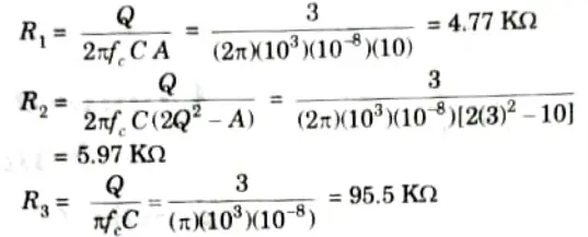
Q11. Design a multiple feedback narrow band pass filter with fc = 1 KHz, Q = 3 and A = 10.
Ans. Given: fc = 1 KHz, Q = 3 and A = 10
To Design: Multiple feedback narrow band pass filter.
Let C1 = C2 =C= 0.01 μF.
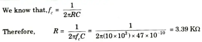
Q12. For a first order Butterworth high pass filter, evaluate the value of R if C = 0.0047 μF and fc = 10 KHz.
Ans. Given: C = 0.0047 μF, fc = 10 KHz
To Find: R.
Unit-III: Frequency Compensation and Non-Linearity (Short Question)
Q1. Write the types of frequency compensation.
Ans. There are two types of frequency compensation:
- i. Internal frequency compensation.
- ii. External frequency compensation.
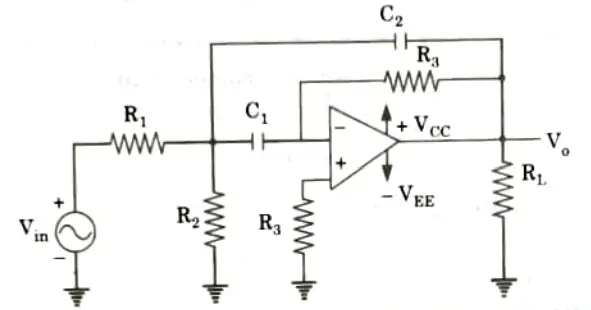
Q2. Draw the circuit diagram of logarithmic amplifier.
Ans.
Q3. Give two applications of analog multiplier.
Ans. i. Frequency doubling.
ii. Measurement of real power.
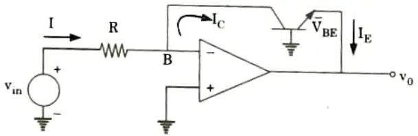
Q4. What is super diode ?
Ans. In order to have a circuit behave like an ideal diode and rectifier, the super diode is amplifier a design obtained with an operational amplifier. It also goes by the name precision rectifier.
Q5. Define comparator and how it is used.
Ans. 1. A comparator is a circuit that contrasts a signal voltage applied to one Op-Amp input with a known reference value applied to the opposite input.
2. The basic comparator can be used as zero crossing detector provided that Vref is 0. It is used as window detector as well as phase meter.
Q6. What is the advantage of precision diode rectifier circuit over ordinary rectifier?
Ans. i. Precision rectifiers are more stable than regular rectifiers
ii. Precision rectifiers are more efficient than regular rectifiers.
Q7. How monostable multivibrator is used ?
Ans. One stable state and one quasi-stable state make up a monostable multivibrator. With the help of a triggering signal, the circuit can produce a single output pulse with a variable duration.
Q8. What do you understand by hysteresis voltage ?
Ans. The voltage at which trigger of pulses occurs from positive level to negative level or vice-versa is known as hysteresis voltage. The hysteresis voltage is equal to the difference between VUT and VLT.
Therefore VH = VUT – VLT
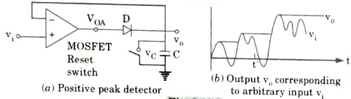
Q9. Name the circuit that is used to detect the peak value of non-sinusoidal waveforms. Explain the operation with neat circuit diagram.
Ans.
- 1. Peak detectors are used to find non-sinusoidal waveforms’ peaks.
- 2. A peak detector’s job is to calculate the input’s peak value. The circuit keeps track of a signal’s voltage peaks and temporarily stores the highest value on a capacitor.
- 3. This updated value is saved if a greater peak signal value appears. Until the capacitor is discharged, the maximum peak value is held.
- 4. When input v1 exceeds v2 the voltage across the capacitor, the diode D is forward biased and the circuit becomes a voltage follower.
- 5. Consequently, the output voltage v0 follows v1 as long as v1 exceeds vc When v1 drops below vc the diode becomes reverse-biased and the capacitor holds the charge till input voltage again attains a value greater than vc.
- 6. Fig. shows the voltage wave shape for the positive peak detector.
Q10. Give the example of a square wave generator which utilizes positive feedback.
Ans. Positive feedback is used in the Schmitt trigger circuit. Schmitt trigger circuits are straightforward positive feedback comparator circuits that turn sinusoidal waves into square waves.
Q11. What is the application of Schmitt trigger ?
Ans. A Schmitt trigger is used to transform an input voltage that changes very slowly into a square wave output.
Q12. What happens to differentiator when it is used at high frequency?
Ans. At high frequencies a differentiator may become more unstable and break into oscillation. The input impedance (1.e., 1/ωc1)decreases with increase in frequency, this making the circuit sensitive to high frequency noise.
Q13. Why the monostable multivibrator also called as gating circuit ?
Ans. The monostable multivibrator is known as a gating circuit because it can be used to gate system components since it produces a rectangular waveform at a set time.
Q14. Write the advantages of negative feedback amplifier.
Ans.
- i. The negative feedback reduces noise.
- ii. It has high stabilized gain.
- iii. It can control step response of amplifier
- iv. It has less harmonic distortion.
Unit-IV: Digital Integrated Circuit Design (Short Question)
Q1. What do you mean by a CMOS circuit logic ?
Ans.
- 1. The CMOS logic gate consists of two networks.
- i. The pull-down network (PDN) constructed of NMOS transistor and
- ii. The pull-up network (PUN) constructed of PMOS transistors.
- 2. The two networks are operated by the input variables, in a complementary fashion.
Q2. Why CMOS NAND is preferred over CMOS NOR?
Ans. The NOR gate will need a lot more space than the NAND gate since the p-region is often two to three times the n-region. The implementation of combinational logic functions in CMOS is therefore preferred to using NAND gates.
Q3. What is threshold voltage ?
Ans. The value of VGS at which a sufficient number of mobile electrons accumulate in the channel region to form a conducting channel is called the threshold voltage.
Q4. What are the advantages of implementing the depletion load NMOS inverter circuit confíguration ?
Ans. i. Sharp VTC transition and better noise margins.
ii. Single power supply. iii.Smaller overall layout area.
Q5. What is PDN and PUN?
Ans. i. Pull up network (PUN): A network that provides a low resistance path to Vdd when output is logic 1 and provides a high resistance to Vdd otherwise.
ii. Pull down network (PDN): A network that provides a low resistance path to ground (GND) when output is logic 0 and provides a high resistance to ground (GND) otherwise.
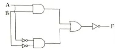
Q6. Implement F = AB+ AB using AND-OR-INVERT logic.
Ans.
Q7. Define the term VIH and VIL for the CMOS inverter.
Ans. A. VIH: VIH is the minimum value of input interpreted by the inverter as a logic 1.
B. VIL: VIL is the maximum value of input interpreted by the inverter as a logic 0.
VIL and VIH are the points on VTC at which the slope is equal to – 1.
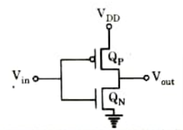
Q8. Draw the basic structure of CMOS inverter.
Ans.
Q9. Define latch.
Ans.
- 1. The simplest memory component is the latch. Two cross-coupled logic inverters make up the device. The inverters create a loop with positive feedback.
- 2. It has two points of operation. With two complimentary outputs, the latch is a bistable circuit.
- 3. A flip-flop is created by the latch and the triggering circuitry.
Q10. Define Fan-in and Fan-out.
Ans. A. Fan-in: The Fan-in of a gate is the number of its inputs. A tour input NOR gate has a Fan-in of 4.
B. Fan-out: Fan-out is the maximum number of Similar gates that a gate can drive.
Q11. How the pull up network can be synthesized ?
Ans. By defining Y as a function of the complemented variables and then applying the uncomplemented variables to the gate of the PMOS transistors, it is possible to directly synthesize the pull-up network.
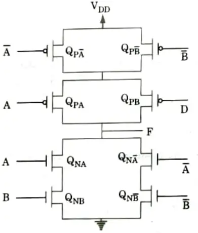
Q12. Implement F = AB+ AB using CMOS.
Ans.
Unit-V: Integrated Circuit Timer (Short Question)
Q1. Define 555 timer and write its applications.
Ans. A. 555 timer: The 555 timer is a very reliable tool for creating precise oscillation or time delay. Microseconds to hours of time delay can be produced by a single 555 timer.
B. Applications:
- i. Pulse generator
- ii. Ramp and square wave generator
- iii. Mono-shot multivibrator
- iv. Burglar alarm
Q2. Describe the need of voltage limiter circuit.
Ans. The voltage level is restricted using a voltage limiter. The voltage limiter is the preferred device when a constant, dependable voltage is required.
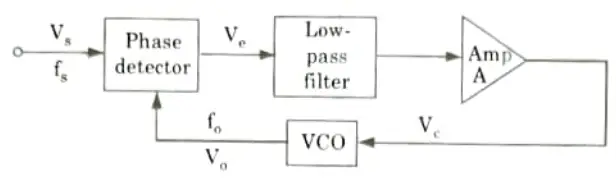
Q3. What are the basic blocks of phase-locked loop?
Ans. 1. PLL stands for Phase Locked Loop. Block diagram of the basic phase locked loop is shown in Fig.
2. PLL consists of :
- i. A phase detector
- ii. Low pass filter
- iii. An erTor amplifier
- iv. Voltage controlled oscillator.
Q4. What is capture range in PlLL ?
OR
Which block of PLL decides capture range ? Explain.
Ans. 1. The input frequency range within which an originally unlocked loop will lock with an input signal is known as the capture range.
2. In PLL, VCO block decides capture range.
Q5. What is the chip number for phase locked loop?
Ans. Chip number of phase locked loop is NE/SE 565.
Q6. Write the applications of PLL.
Ans.
- i. Frequency multiplication/division
- ii. Frequency translation
- iii. AM detection
- iv. FM demodulation
Q7. Write the stages of PLL.
Ans. i. Free running
ii. Capture
iii. Locked or tracing
Q8. Define pull in time.
Ans. Pull in time is the sum of all PLL’s lock-establishing times. The initial phase and frequency offset between the two signals, as well as the general loop gain and loop filter parameters, all play a role in this.
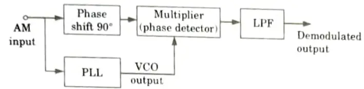
Q9. How the AM detection is used using PLL?
Ans. The AM signal which is to be demodulated is applied to 90° phase shifting network a well as PLL. The phase detector will produce sum and difference of the frequencies at its output.
Q10. Write the applications of monostable modes of 555 timer.
Ans.
- i. Missing pulse detector.
- ii. Linear ramp generator.
- iii. Frequency divider.
- iv. Pulse width modulation.
Q11. Draw the circuit diagram of Schmitt trigger using 555 timer.
Ans.
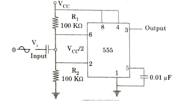
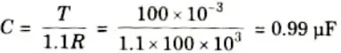
Q12. Calculate the value of C for a monostable multivibrator if R = 100 kΩ and the time delay T = 100 ms.
Ans.
Q13. Write the application of VCO.
Ans. Applications of VCO:
- 1. The various applications of VCO are:
- i. Frequency Modulation.
- ii. Signal Generation (Triangular or Square Wave)
- iii. Function Generation.
- iv. Frequency Shift Keying i.e., FSK demodulator
- v. In frequency multipliers.
- vi. Tone Generation.

Integrated Circuits Btech Quantum PDF, Syllabus, Important Questions
| Label | Link |
|---|---|
| Subject Syllabus | Syllabus |
| Short Questions | Short-question |
| Question paper – 2021-22 | 2021-22 |
Integrated Circuits Quantum PDF | AKTU Quantum PDF:
| Quantum Series | Links |
| Quantum -2022-23 | 2022-23 |
AKTU Important Links | Btech Syllabus
| Link Name | Links |
|---|---|
| Btech AKTU Circulars | Links |
| Btech AKTU Syllabus | Links |
| Btech AKTU Student Dashboard | Student Dashboard |
| AKTU RESULT (One VIew) | Student Result |