With Aktu Btech Quantum Notes, learn about VLSI technology. Utilise these essential, commonly asked questions to master important subjects and perform well on tests. Begin today on the path to success! Unit-5 Metallization and Packaging of VLSI Devices
Dudes 🤔.. You want more useful details regarding this subject. Please keep in mind this as well.

Important Questions For VLSI Technology:
*Quantum             *B.tech-Syllabus
*Circulars              *B.tech AKTU RESULT
* Btech 3rd Year   * Aktu Solved Question Paper
Q1. Explain metallization.
Ans.
- 1. Metallization use in bipolar devices is similar to that in MOSFET.
- 2. In a bipolar transistor, the central region is the semiconductor (base), and is directly in contact with the metal.
- 3. The two neighbouring region are now called emitter and collector, and are also directly in contact with metal.
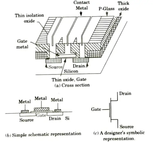
- 4. The metal work function plays an important role in all three regions in determining the current flow characteristics, in a manner similar to that in the source and drain regions of the MOSFET.
- 5. Primary metallization application can be divided into three groups:
- i. Gate,
- ii. Contact, and
- iii. Interconnects.
- 6. Gate metallization and interconnection metallization are both processes that use fine-line metal patterns to connect a large number of MOSFETs or bipolar devices.
- 7. Contact metallization refers to all metalization that is in direct contact with a semiconductor. As was already noted, the metallization method employed for gate and connectivity MOS devices has been polysilicon film.
- 8. Aluminum has been employed as a second-level link to the outside world and as the contact metal on gadgets.
- 9. Many different metallization strategies to create ohmic connections to semiconductors have been suggested.
- 10. A multiple-layer construction with a diffusion barrier has been suggested in a number of situations.
- 11. Platinum silicide (PtSi) has been used as a Schottky barrier contact and also simply as an ohmic contact for deep junctions.
- 12. Titanium/platinum/gold or titanium/palladium/gold beam lead technology has been successful in providing high-reliability connection to the outside world.
Q2. Explain the types of physical vapor deposition.
Ans. There are two types of physical vapor deposition methods:
i. Evaporation:
- 1. In the evaporation process, a film is created when vapour condenses on a substrate that is kept at a lower temperature than the vapour itself.
- 2. When heated to a suitable temperature, all metals evaporate. To reach these temperatures, a variety of techniques can be used, including resistive heating, induction heating, electron bombardment, and laser heating.
- 3. The use of an electron gun for evaporation of transition metals, particularly the refractory metals, is quite widespread.
- 4. E-gun evaporations, on the other hand, result in radiation damage. however, this can be eliminated by high temperature post-deposition heat treatments.
- 5. This approach has the benefit that gas entrapment in the film is little or nonexistent because evaporations occur at pressures that are far lower than sputtering pressures.
- 6. Using two or more independently controlled evaporation sources, the evaporation method can also be utilised to deposit an alloy or a mixture of two or more materials.
- 7. Under independent experimental conditions, the component-specific evaporation rates are calculated. Following that, the environment is changed to deposit an alloy or combination with the required composition.
- 8. Nevertheless, this coevaporation technique, which has been utilized to deposit refractory silicides, calls for good calibration that must be kept both during and between runs.
- 9. Due to fractionation that takes place as the evaporation process continues, coevaporation from a single source containing the alloy elements is typically not feasible.
ii. Sputtering:
- 1. In the process of sputter deposition, intense ions hit the target material to liberate certain atoms. Then, to create a film on the substrate, these atoms are condensed.
- 2. Any materials, including metals, alloys, semiconductors, and insulators, can be sputtered using techniques that are very well regulated and broadly applicable.
- 3. Metal can be deposited via radio frequency, DC, and DC-magnetron sputtering. Due to the fact that the composition of the film is locked to the composition of the target, alloy-film deposition by sputtering from an alloy target is achievable.
- 4. This is accurate even when the puttering rates of the alloy components differ noticeably.
- 5. The component with a high sputtering rate is sputtered off the target preferentially in the early stages of the process. leaving this component lacking on the target surface.
- 6. Deposits with a target-like composition result from the deficient region s50on becoming deficient enough to offset the increased sputtering rate.
- 7. The equipment type, the sputtering conditions, and the alloy component all affect how the target and film compositions differ.
- 8. Many complicated alloys have been deposited with similar compositions in the target and the film by using the right equipment and sputtering conditions.
- 9. By using individual component targets, alloys can also be deposited with perfect compositional control.
- 10. In some circumstances, sputtering the metal in a reactive atmosphere can be used to deposit the compounds.
- 11. As a result, the sputtering chamber can be used to deposit carbide, nitride, and boride using gases like methane, ammonia or nitrogen, and diborane. This process is known as reactive sputtering.
Q3. What do you mean by sputtering ? Explain sputtering yield. Draw the schematic diagram of signal parallel-plate sputtering system and its working.
Ans. A. Sputtering: Sputtering is a widely used technique to fabricate thin film coatings.
B. Sputtering Yield:
- 1. It is described as the quantity of surface atoms that are expelled for each incoming ion at a specific ion energy.
- 2. Yield plots have been established for numerous ion-surface combinations.
- 3. The ion flow angle affects the sputtering yield.
- 4. Because fewer collisions close to the surface are necessary to expel an atom, the maximum sputtering yield occurs as the flux angle is moved away from the surface normal.
C. Parallel-plate sputtering system:
- 1. A geometry used for plasma/cathode sputtering is the parallel-plate configuration, the RP glow discharge version of which illustrated in Fig.
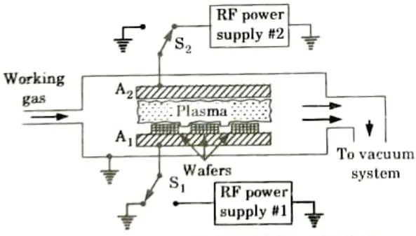
- 2. For sputter deposition of workpieces, the upper electrode is energized by RP.
- 3. A sufficiently high sheath voltage to cause sputtering of this electrode can be maintained in following two ways
- a. One method is by a negative DC bias on the electrode imposed by a separate power supply.
- b. i. The second approach involves maintaining a significant ratio between the areas of the grounded electrode and the energized electrode, on which the workpieces are attached. Sputtered atoms pass through the RF glow discharge plasma in this setup and are deposited on objects positioned on the opposite grounded electrode.
- ii. While this arrangement can work at higher plasma densities, it is more difficult to achieve sheath potentials that are high enough to generate meaningful sputtering rates.
Q4. Explain why sputtering is needed for the deposition of refractory materials like trantalum.
Ans.
- 1. Thin film resistors can be made using refractory metals like tantalum because of their high resistivity and low temperature coefficient of resistance. Tantalum is created via diode sputtering in an inert atmosphere alone.
- 2. However, residual gases in the vacuum chamber such as O2, N2, CO, and CH4 are a source of impurities that lead to the formation of different phases.
- 3. These contaminants influence resistivity, but they are not always bad.
- 4. Tantalum nitrides can actually produce outstanding resistance characteristics.
- 5. Bias sputtering improves control over the purity of tantalum resistors, but it is impossible to avoid stoichiometry errors while creating oxide dielectrics.
Q5. Explain the concept of vacuum deposition.
Ans. 1. The arrangement of metallization process using vacuum deposition technique is shown in Fig.
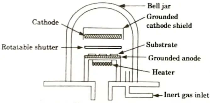
- 2. The silicon wafers are placed face down around the bell jar, with the source of metal in the centre.
- 3. The vacuum pressure is lowered to below 5x 10⁻⁶ Torr before the metal deposition commences.
- 4. The deposited metal subsequently chemically reacts with the silicon dioxide and adheres to the wafer surface as a result of the silicon being heated to a temperature range of 100 to 300°C.
- 5. Upward evaporation is also employed to stop contaminants from dropping onto the wafers that could be produced by the heat source.
- 6. The metal film is normally of 1 𝛍m thickness. The thickness can be monitored by including a quartz crystal oscillator in the vacuum. whose frequency can be set with the amount of metal to be deposited on its surface.
- 7. The wafers are heated at around 1500°C in an inert gaseous environment (for example, nitrogen) following evaporation. Due to this, the metal and silicon surface effectively alloy, resulting in low resistance at the interface between the two. Known as a low ohmic contact joint, this is.
Q6. Discuss and describe the various process design consideration of VLSI devices.
Ans. 1. The VLSI IC circuits design flow is shown in the Fig. The various levels of design are numbered and the blocks show processes in the design flow.
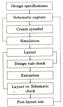
- 2. The functionality, interface, and architecture of the digital IC circuit to be designed are described informally in the specification, which comes first.
- 3. Following the creation of the behavioural description, the design is examined for functionality, performance, adherence to predetermined standards, and other requirements.
- 4. HDLs are used for RTL description. To evaluate functionality, this RTL description has been emulated. We now require the assistance of EDA tools.
- 5. Using logic synthesis tools, the RTL description is subsequently transformed into a gate-level netlist. A gate level netlist is a description of the circuit’s gates and connections in terms of how well they adhere to timing, power, and area requirements.
- 6. Finally, a physical layout is made, which will be verified and then sent to fabrication.

VLSI Technology Btech Quantum PDF, Syllabus, Important Questions
| Label | Link |
|---|---|
| Subject Syllabus | Syllabus |
| Short Questions | Short-question |
| Question paper – 2021-22 | 2021-22 |
VLSI Technology Quantum PDF | AKTU Quantum PDF:
| Quantum Series | Links |
| Quantum -2022-23 | 2022-23 |
AKTU Important Links | Btech Syllabus
| Link Name | Links |
|---|---|
| Btech AKTU Circulars | Links |
| Btech AKTU Syllabus | Links |
| Btech AKTU Student Dashboard | Student Dashboard |
| AKTU RESULT (One VIew) | Student Result |