
Quantum Notes’ essential, commonly asked questions can help you prepare for the Aktu Btech Microprocessor and Microcontroller exam. Improve your comprehension to perform better on your examinations right away! Unit-5 Assembly Programming and Instruction of 8051
Dudes 🤔.. You want more useful details regarding this subject. Please keep in mind this as well.

Important Questions For Microprocessor and Microcontroller:
* Aktu Quantum          * B.tech-Syllabus
* Circulars                     * B.tech AKTU RESULT
* Btech 3rd Year          * Aktu Solved Question Paper
Q1. How an assembly language program is created, assembled and made ready to run ?
Ans. 1. The steps that illustrate how an assembly language program is created assembled and made ready to run is given in the Fig.
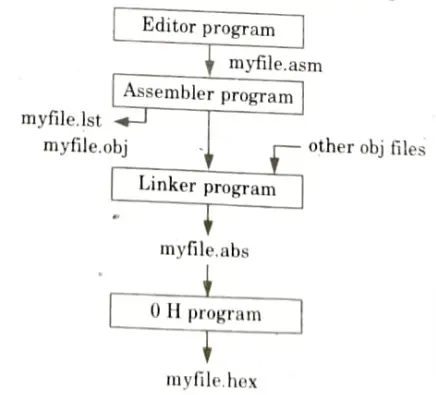
- Steps 1:
- i. To start, the programme is created or edited using an editor. The MS-DOS edit software (or notepad in Windows), which is included with all Microsoft operating systems, is a commonly used editor.
- ii. The editor needs to be capable of creating an ASCII file. Several assemblers use the standard DOS practise for file names, but the source files have the “asm” or “src” extension, depending on the assembler you are using. For the convention, check your assembler.
- iii. An assembler uses the source file’s “asm” extension in the following step.
- Steps 2: An 8051 assembler receives the “asm” source file containing the programme code generated in step 1. The instructions are changed into machine code by the assembler. Both an object file and a list file will be generated by the assembler. The list file’s extension is “1st,” whereas the object file’s extension is “obj.”
- Steps 3: Linking is a necessary third step for assemblers. With the help of one or more object files, the link software creates an absolute object file with the “abs” extension. Trainers for the 8051 that have a monitor software use this abs file.
- Steps 4: Next the “abs” file is fed into a program called “0 H” (object to hex converter), which creates a file with extension “hex” that is ready to burn into ROM. This program comes with all 8051 assemblers.
asm and obj files:
- 1. The “asm” file is also called the source file and for this reason some assemblers require that this file have the “src” extension.
- 2. The 8051 assembler converts the asm file’s assembly language instructions into machine language and provides the obj (object) file.
Ist (list) file:
- 1. The first (list) file, which is optional, contains a list of all the addresses and opcodes as well as any faults that the assembler found. This list is highly helpful to programmers.
- 2. A lot of assemblers make the assumption that the list file is not required unless you explicitly request its production.
- 3. An editor like DOS EDIT can read this file and display it on the screen or print a hard copy by sending it to the printer.
- 4. To discover syntax errors, the programmer consults the list file.
- 5. The obj file is not ready to be entered into the linker programme until all of the errors in the first file have been corrected.
Q2. What do you mean by logical instructions?
Ans. The logical instructions are:
1. AND: The result of this instruction will be placed in the destination after performing a logical AND on the two operands. Often, the accumulator serves as the destination. The source operand may be an immediate, register, or memory-based operand.
Format: ANL destination, source.
For example:
ANLA, R2 ;
2. OR: The source and destination operands are ORed, and the outcome is added to the destination. Some bits of the operands can be set to 1 using the ORL instruction. Often, the accumulator serves as the destination. The source operand may be an immediate, register, or memory-based operand.
Format: ORL destination, source
For example: ORL C, ACC 7;
3. XOR: The XOR operation will be applied to the two operands by this instruction, and the result will be written to the destination. Often, the accumulator serves as the destination. The source operand may be an immediate, register, or memory-based operand.
Format: XRL destination, source
For example: XRL A, # 78 H
4. CPLA (complement accumulator): This instruction complements the contents of register A. The complement action changes the 0s to 1s and the 1s to 0s. This is also called 1’s complement.
Format: CPLA
For example: MOV A, # 55H
CPL A ; now A = AA H
Q3. Timer-0 of 8051 microcontroller is to be programmed in mode-1 for creating a square wave of duty cycle 50 % on the port P1. 5. Write an algorithm for programming the counter.
Ans. A. Program:
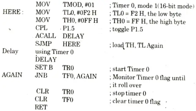
B. Algorithm:
- 1. TMOD is loaded.
- 2. FFF2 His loaded into TH0- TL0.
- 3. P1.5 is toggled for the high and low portions of the pulse.
- 4. The DELAY subroutine using the timer is called.
- 5. In the DELAY subroutine, Timer 0 is started by the SETB TRO instruction.
- i. Timer 0 counts up with the passing of each clock, which is provided by the crystal oscillator. As the timer counts up, it goes through the states of FFF3, FFF4, FFF5, FFF6, FFF7, FFF8, FFF9, FFFA, FFFB, and so on until it reaches FFFFH.
- ii. One more clock rolls it to 0, raising the timer flag (TF0 = 1). At that point, the JNB instruction falls through.
- iii. Timer 0 is stopped by the instruction CLR TRO. The DELAY subroutine ends and the process is repeated.
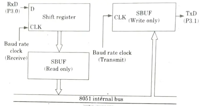
Q4. Explain how serial communication takes place in 8051. State special function registers used for serial communication in 8051 microcontroller.
Ans.
- 1. The 8051’s serial port is full duplex, which allows for simultaneous transmission and reception. It stores data in register SBUF. Data transmission is governed by register SCON, data rates by register PCON, and data transfer via pins RxD (P3.0) and TxD (P3.1).
- 2. On the 8051, SBUF is an 8-bit register reserved for serial communication. It may be found at 99 H. It can be addressed in 8051 just like any other register.
- 3. Writing to SBUF loads data to be transmitted and reading SBUF accesses received data.
- 4.There are two separate and distinct register, the transmit write-only register, and the receive read-only register. This is shown in Fig.
- 5. The way in which SBUF is used for the transmission and reception of the data during serial communication is explained below:
- a. Transmission: When a byte of data is to be transmitted via the TxD pin, the SBUF is loaded with this data byte. As soon as a data byte is written into SBUF, it is framed with the start and stop bits and transmitted serially via the TxD pin.
- b. Reception: When 8051 receives data serially via RxD pin of it, the 8051 deframes it. The start and stop bits are separated out from a byte of data. This type is placed SBUF register.
Q5. Discuss the key press and key detection mechanism of keyboard.
Ans.
- 1. Keyboards are organized in a matrix of rows or columns.
- 2. The CPU accesses both rows and columns through ports; thus, with two 8-bit ports, an 8 x 8 matrix af keys can be connected to a microprocessor. When a key is pressed, a row and a column make a contact.
- 3. To understand the mechanism let us consider a 4 x 4 matrix connected to two ports as shown in Fig.
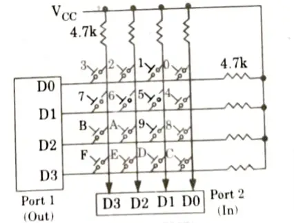
- 4. The rows are connected to an output port and the columns are connected to an input port.
- 5. If no key has been pressed, the input port will yield ls for all columns since they are all connected to high (VCC).
- 6. If all the rows are grounded and a key is pressed, one of the columns will have 0 since the key pressed provides the path to ground.
- 7. It is the function of the microcontroller to scan the keyboard continuously to detect and identify the key pressed.
- 8. To detect a pressed key, the microcontroller ground all rows by providing 0 to the output latch, then it reads the columns. If the data read from the columns is D3-D0 = 1111, no key has been pressed and process continues until a key press is detected.
- 9. However, if one of the column bits has a zero, this means that a key press has occurred.
- 10. For example, if D3-DO = 1101, this means that a key in the Dl column has been pressed. After a key press is detected, the microcontroller will go through the process of identifying the key.
- 11. The microcontroller grounds it by giving a low to row DO alone, then reads the columns, starting with the top row.
- 12. If all of the data read is correct, the process moves on to the following row and no key in that row is activated. It scans the columns, grounds the following row, and looks for any zeros. Up till the row is found, this process is repeated.
- 13. The next job is to determine which column the pushed key belongs to after determining the row in which it was pressed.
- 14. Since the microcontroller always knows which row and column are being accessed, this should be simple.
Q6. How many interrupts in 8051 ? Also draw interrupt vector table for the 8061.
Ans. The six interrupts in the 8051 shown in Table.
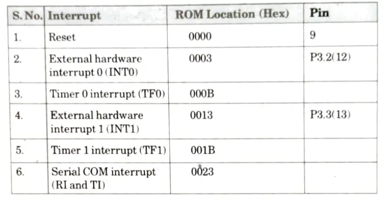
- 1. Reset: When the reset pin is activated, the 8051 jumps to address location 0000.
- 2. The timers will each have two interrupts: one for timer 0 and one for timer 1. The interrupt vector table’s memory addresses 000BH and 001BH, which correspond to timers 0 and 1, respectively.
- 3. Two interrupts are set aside for hardware external hardware interrupts. in numbers 12 (P3.2) and 13(P3.3) in port 3 are for the external hardware interrupts INTO and INT1 respectively. These external interrupts are also referred to as EX1 and EX2.
- 4. In serial communication, the same interrupt is used for send and receive. This interrupt is associated with the interrupt vector table address 0023H.

Microprocessor and Microcontroller Btech Quantum PDF, Syllabus, Important Questions
| Label | Link |
|---|---|
| Subject Syllabus | Syllabus |
| Short Questions | Short-question |
| Question paper – 2021-22 | 2021-22 |
Microprocessor and Microcontroller Quantum PDF | AKTU Quantum PDF:
| Quantum Series | Links |
| Quantum -2022-23 | 2022-23 |
AKTU Important Links | Btech Syllabus
| Link Name | Links |
|---|---|
| Btech AKTU Circulars | Links |
| Btech AKTU Syllabus | Links |
| Btech AKTU Student Dashboard | Student Dashboard |
| AKTU RESULT (One VIew) | Student Result |