
Table Of Contents
Boost your Aktu Btech Microprocessor and Microcontroller preparation with Quantum Notes’ essential, commonly asked questions. Improve your understanding and excel in your tests today! Unit-1 Introduction to Microprocessor
Dudes 🤔.. You want more useful details regarding this subject. Please keep in mind this as well.

Important Questions For Microprocessor and Microcontroller:
* Aktu Quantum          * B.tech-Syllabus
* Circulars                     * B.tech AKTU RESULT
* Btech 3rd Year          * Aktu Solved Question Paper
Q1. Explain various types of microprocessor (𝜇P).
Ans. A. 8085 microprocessor:
- 1. The 8085 CPU is the most popular CPU.
- 2. The 8085, which is an 8-bit Microprocessor. The CPU has an on-chip clock generator and performs well with a decent optimal register configuration and a moderately powerful ALU.
- 3. Addressing capacity, sluggish memory speed of scratchpad registers and execution, a restricted number of unavailable compiler instruction sets, and addressing modes are the main limitations of this 8-bit microprocessor.
B. 8086 microprocessor:
- 1. Intel’s initial 16-bit CPU was the outcome of the designer’s efforts to create a more potent and effective computer.
- 2. The 8086 has a broad instruction set, 16-bit ALU support, a set of general-purpose registers, and a segmented memory addressing system.
- 3. The inclusion of a set of segment registers in the 8086 for addressing segmented memory was in fact a significant development in the assessment process.
- 4. The lack of memory management and protection features was the 8086’s main drawback.
C. 80286 microprocessor:
- 1. The 80286 was the first Microprocessor to provide memory management, privilege, and protection capabilities.
- 2. Nonetheless, the maximum segment size that the 80286 Processor could tolerate was constrained.
- 3. Another drawback of the 80286 was that it was challenging to return it to real mode after switching it to protected mode.
- 4. Resetting the system was the only method to return it to the real mode.
D. 80386 microprocessor:
- 1. 80386 was the first 32-bit CPU from Intel.
- 2. The 80386’s memory management capabilities were improved to handle paging, virtual memory, and four layers of security.
- 3. The maximum segment size in the 80386 architecture was increased and now goes up to 4 GB.
- 4. The 80386 and its 80387 math coprocessor provide a fast environment.
E. 80486 microprocessor :
- 1. The 80486 was designed with an integrated math coprocessor.
- 2. After getting integrated, the speed of execution of mathematical operations enhanced three folds.
- 3. Also for the first time, an 8 KB four-way set associative code and data cache was introduced in 80486.
- 4. A five stage instruction pipeline was also introduced.
F. Pentium microprocessor:
- 1. Its architecture is super scalar and super pipelined.
- 2. It has two integer pipelines, U and V, each of which has four stages.
- 3. The floating point performance has improved thanks to an on-chip floating point unit.
- 4. The following Pentium iteration is Pentium-II.
- 5. It has a sizable cache and includes every Pentium-Pro capability.
- 6. The 0.25 microtechnology-based Pentium-III contains more than 9.5 million transistors.
Q2. Explain the microprocessor architecture and operation of its components.
Ans. A. Architecture:
- 1. For the efficient flow of data and results from one functional block to the next, microprocessor architecture specifies the proper placement of its numerous functional blocks in the form of necessary circuitry.
- 2. The most general purpose architecture of microprocessor is shown in Fig.
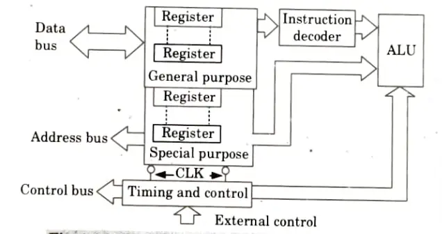
B. Components:
- 1. ALU (Arithmetic logical unit): It is made up of a shift register, a status register, an accumulator, an adder, and temporary registers. Several arithmetic and logical operations are carried out by this ALU unit.
- 2. General purpose register: When used in register pair mode, the microprocessor’s 8-bit general purpose registers can be used as 16-bit register pairs. They are used to store both the address and data.
- 3. Special purpose register: This consists of an accumulator, a programme counter, a stack pointer, and a register for status flags. These registers are employed in a few particular situations that the manufacturers have specified.
- 4. Instruction decoder: This takes the information from the instruction register and creates the control signals that open the data pathways required to carry out the instruction.
- 5. Timing and control unit:
- i. All processes inside and outside the microprocessor are coordinated and controlled by this device.
- ii. The master clock is the source of the timing and control signals that govern the system transfers and transformations related to each instruction.
- iii. The control unit also takes control signals produced by other microprocessor system-related devices.
- 6. Address bus: This is employed to send address data. To support addressing and the capacity to address up to 64 KB of memory, the 6. address bus typically has 16 bits.
- 7. Control bus: The synchronization signals are carried on a variety of single lines in this. Such lines are used by the CPU to supply timing signals.
Q3. List the four operations commonly performed by the MPU.
Ans.
- 1. The four operations commonly performed by the microprocessor (MPU) are as follows:
- i. Memory read: Reads data (or instructions) from memory.
- ii. Memory write: Writes data (or instructions) into memory.
- iii. I/O read: Accepts data from input devices.
- iv. I/O write: Sends data to output devices.
- 2. All these operations are part of the communication process between the MPU and peripheral devices.
- 3. To communicate with a peripheral (or a memory location), the MPU needs to perform the following steps:
- i. Identify the peripheral or the memory location (with its address).
- ii. Transfer binary information (data and instructions).
- iii. Provide timing or synchronization signals.
Q4. What is transparent latch, and why it is necessary to use a latch with output device ?
Ans.
- 1. A latch is a D flip-flop. Two types of D flip-flops are available, a transparent latch and a positive-edge-triggered flip-flop.
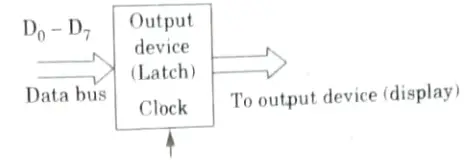
- 2. When the clock signal is high, a transparent latch adjusts its output in accordance with the input D.
- 3. The output Q will latch (keep) the most recent value of the input D when the clock signal becomes low.
- 4. The simplest kind of output port is the latch.
- 5. A latch connects the output device to the microprocessor.
- 6. The microprocessor latches the data from the data bus to the output of the latch when it wishes to send the data to the output device. This is done by activating the clock signal of the latch.
- 7. The output device can then access it at the latch’s output.
- 8. To hold the output data for display, a latch is utilized for an output port; however, the input data byte is received by turning on a tri-state buffer and is then stored in the accumulator.
Q5. What is function of accumulator ?
Ans. A. Importance of ALE:
- 1. ALE is used to indicate the beginning of any operation.
- 2. It is a positive going pulse used primarily to latch lower order address from multiplexed bus (AD0 – AD7) and generate separate set of eight address line (A0 – A7).
B. Importance of ALU:
- 1. As implied by its name, the ALU performs arithmetic and logical operations.
- 2. The CU (Control Unit) sends the necessary operands to the ALU for processing, which then sends them to registers to be saved and displayed for the user to see on the screen.
C. Function of accumulator (ACC):
- 1. The accumulator is an 8-bit register associated with the ALU.
- 2. The register A in the 8085 is an accumulator.
- 3. It is used to hold one of the operands of an arithmetic or logical operation.
- 4. It serves as one input to the ALU.
- 5. The other operand for an arithmetic or logic operation may be stored either in the memory or in one of the general-purpose registers.
- 6. The final result of an arithmetic or logical operation is placed in the accumulator.
Q6. Write short note on logic devices for interfacing.
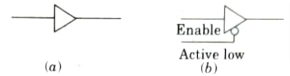
Ans. A. Tri-state devices:
- 1. These are the devices which have three logic states; i.e., logic 0, logic 1 and high input impedance.
- 2. When these devices’ enable lines are active, they function as normal logic devices; however, when the enable lines are inactive, the logic devices transition to a high-impedance condition and act as though they are detached from the system.

B. Buffer:
- 1. The circuit, which amplifies the current or power, is logical. Both the input and output lines are single.
- 2. It applies the same amount of logic to the output as it does to the input.
- 3. Typically, it is employed to enhance the logic circuit’s driving capacity; therefore, the term “driver.”
- 4. Fig. shows a diagram of tri-state buffer. In this buffer, when enable line is low then it behaves as buffer: otherwise it remains in high impedance state.
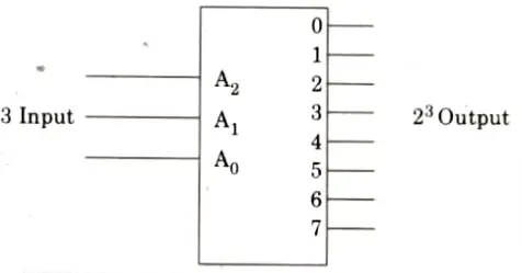
C. Decoder:
- 1. Decoder is a logic circuit that identifies combination of signals that are applied at the input.
- 2. In decoder if there are n input lines then at the output there are 2n output lines.
- 3. Suppose there is 3 x 8 decoder, i.e., there are 3 input lines then there are 28,i.e., 8 possible combination which are identified by 0 to 7 output lines.
- 4. If 111 is applied at the input then the output at 7 will be 1 and all others will remain at logie zero.
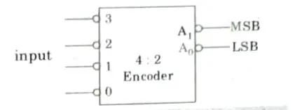
D. Encoder:
- 1. When a signal is applied at the input, an encoder, which is a logic circuit, outputs the proper code for each of the applied signals. It is the decoding process done backwards.
- 2. In the encoder, there are 2n input lines and n output lines.
- 3. Assume that a signal is applied at input 3 and that both the LSB and MSB go high at the output.
- 4. In a similar manner, the MSB goes high and the LSB goes low when the signal is presented to input 2.
- 5. Nevertheless, when two or more lines are triggered concurrently at once, this encoder is unable to deliver proper code at the output.

Microprocessor and Microcontroller Btech Quantum PDF, Syllabus, Important Questions
| Label | Link |
|---|---|
| Subject Syllabus | Syllabus |
| Short Questions | Short-question |
| Question paper – 2021-22 | 2021-22 |
Microprocessor and Microcontroller Quantum PDF | AKTU Quantum PDF:
| Quantum Series | Links |
| Quantum -2022-23 | 2022-23 |
AKTU Important Links | Btech Syllabus
| Link Name | Links |
|---|---|
| Btech AKTU Circulars | Links |
| Btech AKTU Syllabus | Links |
| Btech AKTU Student Dashboard | Student Dashboard |
| AKTU RESULT (One VIew) | Student Result |