
Learn about B.Tech AKTU Quantum Book Short Question Notes on Microprocessor and Microcontroller. Explore the realm of programming, interfaces, and embedded systems for cutting-edge applications.
Dudes 🤔.. You want more useful details regarding this subject. Please keep in mind this as well.

Important Questions For Microprocessor and Microcontroller:
* Aktu Quantum          * B.tech-Syllabus
* Circulars                     * B.tech AKTU RESULT
* Btech 3rd Year          * Aktu Solved Question Paper
Unit-I: Introduction to Microprocessor (Short Question)
Q1. Define microprocessor, computer and microcontroller.
Ans. A. Microprocessor: The term “microprocessor” refers to a variety of multipurpose, programmable, clock-driven, register-based electronic devices. These devices read binary instructions from a memory storage device, accept binary data as input, process the data in accordance with instructions, and output the results.
B. Computer: It is possible to programme a computer. It consists of I/O (input/output) devices, memory, and microprocessors.
C. Microcontroller: A VLSI-fabricated device with a microprocessor, memory, and I/O signal lines all on the same chip.
Q2. What are the various operations performed by microprocessor ?
Ans. Operations performed by microprocessor:
- 1. Microprocessor initiated operation
- 2. Internal operation
- 3. Peripheral operation
Q3. Explain the significance of HOLD and READY pin of 8085 microprocessor.
Ans. A. HOLD (Pin 39): DMA functioning requires the presence of this pin. Any input/output device that places a high condition (1) on this pin denotes that the data is prepared for DMA transfer.
B. READY (Pin 35): It indicates to microprocessor to wait for time the data become available, with READY = 0 microprocessor waits till READY = 1. At READY = 1, the microprocessor knows that the data is available from memory or I/O devices.
Q4. Give the set of registers involved in 8085 microprocessor.
Ans.
- i. General purpose register
- ii. Temporary register
- iii. Special purpose register
- iv. Sixteen bit register
Q5. Write the use of memory of microprocessor.
Ans. Memory is used to store binary instruction and data for the microprocessor.
Q6. Calculate the address lines required for an 8 Kbyte memory chip.
Ans. 1. 8 Kbyte = 8192 byte
2. Number of address lines,
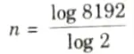
= 13 address lines
Q7. Calculate number of memory chip needed to design 8 Kbyte memory, if the memory chip size is 1024 x 1.
Ans. 1. The chip 1024 x 1 has 1024 (1K) registers and each register can store 1 bit.
2. For 8 Kbyte,
(8 x 1024) ÷ (1024 x 1) = 8 chips
Q8. Give the description of Address Latch Enable (AlLE) signal.
Ans. 1. Every time the 8085 starts an operation, an ALE pulse that is positive and giving is generated.
2. It indicates that the bits on AD7 – AD0 are address bits. It is used to latch the low order address from the multiplexed bus.
Q9. What is the purpose of tri-state logic device ?
Ans. Tri-state logic devices are necessary for a bus-oriented system to operate properly, when multiple components use the same bus lines. It has three states: high impedance, logic 1, and logic 0.
Q10. What is the objective of interfacing an output device?
Ans. In order to get data or a result out of the processor and store it or display it, an output device needs to be interfaced.
Q11. Give the types of interfacing input/output devices.
Ans. There are two types of interfacing input/output devices.
- i. Peripheral I/O
- ii. Memory mapped I/O
Q12. Give any two difference between memory-mapped I/O and peripheral I/O.
Ans.
| S. No. | Memory-mapped I/O | Peripheral I/O |
| 1. | Address is of 16-bit. | Address is of 8-bit. |
| 2. | Data transfer takes place between register and I/O device. | Data transfer take place between I/O and accumulator. |
Q13. What is the maximum number of input devices that can be connected to 8085 in memory mapped I/O?
Ans. The maximum number of input devices that can be connected to 8085 in memory mapped 10 are 65536 (216).
Q14. Discuss the interfacing of DIP switches as an input device.
Ans. With the exception of bus signals and circuit components, input device and output device interfaces are equivalent. The 3:8 decoder may interface an eight DIP switch.
Unit-II: Basic Programming Concepts (Short Question)
Q1. Describe briefly the concept of flow chart.
Ans. A programmer utilizes it as a visual representation when deciding how to approach an issue.
Q2. Discuss the data transfer operation.
Ans. The data transfer operation copies data from a source register or memory location to a destination register or memory location.
Q3. List down the various data transfer operation.
Ans.
- i. MOV (Move)
- ii. MVI (Move immediate data)
- iii. LXI(Load register pair immediate)
- iv. LDA (Load accumulator direct)
- v. SHLD (Store H and Lregister direct)
- vi. STAX (Store accumulator indirect)
Q4. Write instructions to read the data at input port 07 H and at the port 08 H. Display the input data from 07 H at output port 00 H and store the input data from port 08 H in register B.
Ans. IN 07H
OUT 00 H
IN 08 H
MOV B, A
Q5. Write down the various arithmetic operations.
Ans.
- i. ADD (Add register to accumulator)
- ii. ADI (Add immediate to accumulator)
- iii. SUB (Subtract the number)
- iv. SUI (Subtract immediate from accumulator)
- v. INR (Inerement content by 1)
- vi. DCR (Decrement content by 1)
Q6. What operation can be performed by using the instruction SUB A ? Specify the states of Z and CY.
Ans. The instruction SUB A will clear the accumulator.
The flag status will be : CY = 0, Z = 1.
Q7. Write down the various logical instructions.
Ans.
- i. ANA (Logical AND with accumulator)
- ii. ANI (AND immediate with accumulator)
- iii. XRA (Exclusive OR with accumulator)
- iv. XRI (Exclusive OR immediate with accumulator)
- v. ORA (Logically OR with accumulator)
- vi. ORI (Logically OR immediate with accumulator)
Q8. Describe the following 8085 instructions:
i. DAA
ii. JPE 3040 H
Ans. i. DAA (Decimal adjust accumulator): The result of adding two packed BCD numbers is converted into a valid BCD number using this instruction.
ii. JPE3040 H: Jump to the address 3040 Hif parity is even.
Q9. Differentiate between the types of loops.
Ans. Loops are classified as continuous loop and conditional loops.
Difference:
| S. No. | Continuous loop | Conditional loop |
| 1. | Instructions to jump unconditionally are present in continuous loop. Unless the system is reset, a programme containing this kind of loop does not terminate. | Conditional jump instructions are used to create conditional loops. |
Q10. Write short note on counter.
Ans. The fundamental purpose of counters is to record events. It is possible to use INR or DCR instructions to count after loading the proper number into any one register of the CPU.
Q11. Describe the delay using one register.
Ans. The instructions are as follows:
MVIC, FFH ; Load register C
Loop: DCR C ; Decrement C
JNZ Loop ; Jump back to decrement C
Q12. What is the difference between hardware interrupts and software interrupts of 8085 microprocessor ?
Ans.
| S. No. | Hardware Interrupt | Software Interrupt |
| 1. | When a hardware interrupt occurs, a peripheral device that is interrupting the primary program’s I/O process is to blame. | The execution of the instruction in a software interrupt is what causes the interruption. These are unique instructions that the CPU supports. |
| 2. | Hardware interrupts are: RST7.5, RST 6.5, RST 5.5, INTR, TRAP. | Software interrupts are: RST 0 to RST 7. |
Q13. Define the RIM and SIM instruction of 8085 microprocessor.
Ans. A. RIM (Reset Interrupt Mask): This instruction is used to read interrupt marks, to identify pending interrupts and to receive serial data.
B. SIM (Set Interrupt Mask): It reads accumulator and enable and disable interrupts according to accumulator content.
Q14. How the microprocessor behaves when the interrupt is generated through interrupt pin of 8085 (TRAP, RST 7.5, RST 6.5, RST 5.5) and DMA interrupt?
Ans. Interrupt pin of 8085:
- a. TRAP: When this interrupt is received the processor saves the contents of the PC register into stack and branches 0024 H.
- b. RST 7.5: When this interrupt is received the processor saves the contents of the PC register into stack and branches to 003C H.
- c. RST 6.5: When this interrupt is received the processor saves the contents of the PC register into stack and branches to 0034 H.
- d. RST5.5: When this interrupt is received the processor saves the contents of the PC register and branches to 002C H.
- e. DMA interrupt: The 8085 has two lines dedicated to DMA operation-the HOLD and HLDA lines. The HOLD line may be used by the I/O devices to receive an acknowledgement to this request.
Unit-III: 16-bit Microprocessor (Short Question)
Q1. Differentiate between 8085 and 8086 microprocessor.
Ans.
| S. No. | 8085 | 8086 |
| 1. | 8-bit microprocessor. | 16-bit microprocessor. |
| 2. | 16 address lines. | 20 address lines. |
| 3. | It does not support pipelining. | It supports pipelining. |
Q2. List the functional units of 8086.
Ans. i. Bus interface unit (BIU)
ii. Execution unit (EU)
Q3. Why there are two ground pins in 8086 ? Explain.
Ans. There are two ground pins in 8086 to distribute power for noise reduction.
Q4. What is the significance of pipelining in 8086 microprocessor ?
Ans. Pipelining is the process of gathering and then executing computer instructions and jobs from the processor. It permits storage. setting priorities, overseeing, and carrying out activities and directives in a systematic manner.
Q5. Explain need of memory segmentation in 8086.
Ans. i. It permits a 1 MB memory addressing capacity despite the fact that each instruction’s address is only 16 bits.
ii. It facilitates use of separate memory areas for program data and stack.
Q6. What is DMA?
Ans. DMA (Direct Memory Access) is an I/O for high technique commonly used speed data transfer.
Q7. List the priority schemes of DMA requests.
Ans. i. Fixed priority scheme.
ii. Rotating priority scheme.
Q8. Explain the significance of status register in 8237.
Ans. All DMA channel pending requests are tracked in the status register, along with the state of each terminal count.
Q9. List any two salient features of mode 2 in 8255.
Ans. i. The 8-bit port is bidirectional and additionally a 5-bit control port is available.
ii. Inputs and outputs are both latched.
Q10. What is 8255?
Ans. The 8255 is a programmable peripheral interface which is used for parallel data transfer.
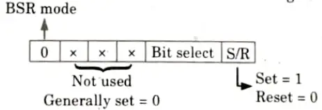
Q11. Write the control word format for BSR mode of 8255.
Ans. Control word format for BSR mode of 8255 is given as:
Q12. What are the basic differences between 8253 and 8254 programmable timer/counter ?
Ans.
| S. No. | 8253 | 8254 |
| 1. | Operating frequency 0-2.6 MHz. | Operating frequency 0-10 MHz. |
| 2. | Read-back command not available. | Read-back command available. |
Q13. What is 8259A?
Ans. A number of interruptions must be handled simultaneously by the programmable interrupt controller 8259A. The priority of interruptions is likewise determined by this controller.
Q14. List any two features available in 8259.
Ans. i. 8259 can be programmed to get 4 priority interrupts.
ii. By cascading 8259, it is possible to get 64 priority interrupts.
Unit-IV: 8051 Microcontroller Basics
Q1. What do you mean by embedded system ?
Ans. 1. An embedded system is an electrical or electromechanical device that combines hardware and firmware to carry out a specific task (software).
2. Each embedded system is distinct, and the software and hardware are both highly specialized for the application domain.
Q2. What are the main application areas of embedded system?
Ans. The main application areas are:
- 1. Consumer electronics: camcorders, cameras etc.
- 2. Household appliances: T.V., fridge etc.
- 3. Telecom
- 4. Healthcare
- 5. Computer peripherals.
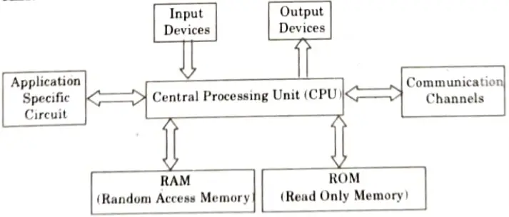
Q3. Draw a basic block diagram of embedded system.
Ans.
Q4. What are the advantages of microcontroller over microprocessor ?
Ans.
- 1. Microcontrollers are normally less expensive than microprocessors.
- 2. It meets the computing needs of the task most effectively.
- 3. Power consumption is low.
- 4. Software piracy can be protected in microcontroller.
Q5. Give the comparison of 8051 family members.
| Feature | 8051 | 8052 | 8031 |
| ROM (on-chip program space in bytes) | 4K | 8K | 0K |
| RAM (bytes) | 128 | 256 | 128 |
| Timers | 2 | 3 | 2 |
| I/O pins | 32 | 32 | 32 |
| Serial port | 1 | 1 | 1 |
| Interrupt sources | 6 | 8 | 6 |
Q6. Compare 8051 and MSP430x5xxx main features.
Ans.
| S. No. | 8051 | MSP430x5xxx |
| 1. | It is 8 bit microcontroller. | It is 16 bit microcontroller. |
| 2. | It is based on CISC architecture. | It is based on RISC architecture. |
| 3. | It has clock frequency of 12 MHz. | It has clock frequency of 3.3 MHz. |
| 4. | It supports 5 addressing modes for source and destination operand. | It supports 7 addressing modes for source operand and 4 addressing modes for destination operand. |
Q7. What are flags available in 8051?
Ans. The flags available in 8051 are: CY (Carry flag), AC (Auxiliary carry flag), OV (over flow flag) and P (Parity flag).
Q8. What do you mean by SFR?
Ans. 1. The 8051 operations that do not use the internal 128-bytes RAM addresses from 00 H to 7FH are done by a group of specific internal register, each called a Special Functions Register (SFR).
2. In 8051, register A, B, PSW and DPTR are a part of the group of registers referred as SFR.
Q9. What is the size of the program counter register ? What does the program counter do ?
Ans. Program counters are 20 bits in size. A register that holds the address of the instruction now being executed is called a programme counter.
Q10. What do you mean by addressing modes ?
Ans. The CPU has a variety of ways to access data. The information might be stored in memory or a register, or it might be given as an immediate value. Hence, addressing modalities refers to the many methods of accessing the data.
Q11. Name the various types of addressing modes used in 8051 microcontroller.
Ans. The 8051 consists of 5 addressing modes:
- 1. Immediate.
- 2. Register addressing mode.
- 3. Register indirect addressing mode.
- 4. Indexed addressing mode.
- 5. Direct addressing mode.
Q12. What is the advantage of register indirect addressing mode over direct addressing mode ?
Ans. The advantage of register indirect addressing mode is that it transforms data access from static to dynamic, as opposed to direct addressing mode’s static approach.
Unit-V: Assembly Programming and Instruction of 8051
Q1. What do you mean by assembly language ?
Ans. A programme written in assembly language is made up of lines of instructions. These commands consist of a mnemonic that may or may not be followed by one or more operands. Operands are the data objects being changed, and mnemonics are the instructions given to the Processor.
Q2. How does an instruction differ from directive ?
Ans.
| S. No. | Instruction | Directive |
| 1. | A mnemonic precedes an instruction, which may be followed by one or more operands. In essence, it instructs the CPU. | Directives provide the assembler with instructions. |
| 2. | To be executed by the CPU, the instructions are converted into machine code (opcode). | Directives are only utilised by the assembler and do not produce any machine code. |
Q3. List the different assembler directives.
Ans. The following are the widely used 8051 assembler directives:
- i. ORG (Origin).
- ii. EQU (Equate).
- iii. END.
- iv. DB (Define byte).
Q4. What do you mean by END directive?
Ans. The END directive informs the assembler that the source (asm) file has ended. An 8051 programme ends with the END directive, therefore anything following that in the source code is disregarded by the assembler.
Q5. Why are the ORG and END directives also called pseudocode?
Ans. 1. ORG and END directives are called pseudocodes because they are directives to the assembler.
2. ORG tells the assembler to place the opcode at memory location 0 while END indicates to the assembler the end of source code.
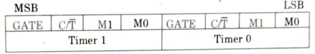
Q6. Draw the structure of TMOD register.
Ans.
Q7. Define the use of MOVX and MOVC instruction in 8051 microcontroller.
Ans. A. MOVX: This instruction transfers data byte between external memory and register.
MOVX destination-byte, source-byte
Example: MOVX A, @ DPTR
MOVX @ DPTR, A
B. MOVC: This instruction moves 1 byte of data located in the program area to A (accumulator). The address of the desired byte of data is formed by adding the program counter (PC) register to the original value of A.
Example: MOVC A, @ A + PC
MOVC A, @ A + DPTR
Q8. Enlist the interrupt in 8051 microcontroller.
Ans.
- i. Reset,
- ii. Timer O’TFO),
- iii. Timer 1(TF1),
- iv. INTO,
- v. INT1,
- vi. Serial COM interrupt (RI and TI).
Q9. Find the timer’s clock frequency and its period for various 8051 based systems, with the following crystal frequency :
a. 12 MHz
b. 16 MHz
c. 11.592 MHz
Ans. a. Timer’s clock frequency = 1/12 x 12 MHz = 1 MHz
and T = 1/1 MHz = 1 μs
b. Timer’s clock frequency = 1/12 x 16 MHz = 1.333 MHz and
T = 1/1.333 MHz = 75 μs
c. Timer’s clock frequency = 1/12 x 11.592 MHz = 921.6 kHz;
T = 1/921.6 kHz = 1.085 μs
Q10. How registers are selected in LCD?
Ans. 1. The RS (Register Select) is used for the selection of registers in LCD.
2. If RS = 0, the instruction command code register is selected.
3. If RS = 1, the data register is selected allowing the user to send data to be displayed on the LCD.
Q11. Define bit addressable RAM in 8051 microcontroller.
Ans. Of the 128 byte internal RAM of the 8051, only 16 byte are bit-addressable. The bit addressable RAM locations are 20 H to 2F H. These 16 bytes provide 128-bits of RAM bit-addressability, since 16 x 8 = 128. They are addressed as 0 to 127 (in decimal) or 00 H to 7 FH.
Q12. What do you understand by stepper motor ?
Ans. The rotor of the stepper or stepping motor moves in distinct steps. The quantity of pulses delivered into the control circuit determines the rotation’s angular angle. Every input pulse starts the driving circuit, which generates an angular movement of one step.

Microprocessor and Microcontroller Btech Quantum PDF, Syllabus, Important Questions
| Label | Link |
|---|---|
| Subject Syllabus | Syllabus |
| Short Questions | Short-question |
| Question paper – 2021-22 | 2021-22 |
Microprocessor and Microcontroller Quantum PDF | AKTU Quantum PDF:
| Quantum Series | Links |
| Quantum -2022-23 | 2022-23 |
AKTU Important Links | Btech Syllabus
| Link Name | Links |
|---|---|
| Btech AKTU Circulars | Links |
| Btech AKTU Syllabus | Links |
| Btech AKTU Student Dashboard | Student Dashboard |
| AKTU RESULT (One VIew) | Student Result |
4 thoughts on “Microprocessor and Microcontroller KEC-502 Btech Aktu Short Question Quantum Book Pdf”