
Quantum Book Pdf of Microprocessor and Microcontroller Important Questions 2022–2023, Solved Question Paper, Repeated Most Important Questions, Syllabus, Aktu Notes
Dudes 🤔.. You want more useful details regarding this subject. Please keep in mind this as well.

Important Questions For Microprocessor and Microcontroller:
* Aktu Quantum          * B.tech-Syllabus
* Circulars                     * B.tech AKTU RESULT
* Btech 3rd Year
Section A: Microprocessor and Microcontroller Aktu Notes Short Questions
a. Discuss the specifications of 8085 microprocessor.
Ans. Specifications of 8085 microprocessor are:
- 1. It is an 8-bit microprocessor.
- 2. It has 16-bit address lines A0 – A15 and hence can point up to 216 = 65535 bytes (64 kB) memory locations.
- 3. It provides 5 level interrupts and supports external interrupt request.
- 4. It performs arithmetic and logical operations.
b. List the disadvantages of memory mapped I/O.
Ans. Disadvantages of memory mapped I/O are:
- 1. There is no separate IN, Out and MOV instruction.
- 2. In memory mapped I/O the same address can’t be assigned to both memory location and I/O devices.
c. State the number of T-states required for following instructions: MVI A, 34 H, LXI H 2000 H.
Ans. i. MVIA, 34 H: 3T states will be required.
ii. LXI H, 2000 H: 10T states will be required.
d. List all the maskable and non-maskable interrupts of 8085.
Ans. A. Maskable interrupts of 8085 are:
- i. RST 7.5
- ii. RST 6.5
- iii. RST5.5
- iv. INTR
B. Non-maskable interrupts of 8085:
- i. TRAP
e. Explain the physical address, offset address and segment address in context to 8086.
Ans. 1. A 20-bit physical address is created by adding the contents of an offset register, also known as an offset address, to the result of shifting the content of a segment register four times left bit-wise to create the physical address.
2. For example, if the segment address is 1005 H and the offset is 5555 H, 2. then the physical address is calculated as follows:
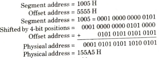
So, 155A5 H is the physical address.
f. Discuss the various memory segments in 8086.
Ans.
- 1. In the segmented addressing, on the other hand, the available memory space is divided into “chunks” called segments. Sucha memory is known as segmented memory.
- 2. In 8086 system the available memory space is 1 Mbytes. This memory is divided into number of logical segments.
- 3. Each segment is 64 Kbytes in size and addressed by one of the segment registers.
g. Explain the organization of stack in 8051.
Ans. Up to 64 K of programme memory and 64 K of data memory are accessible. The internal data 1 memory of the 8051 is 256 bytes, while the internal programme memory is 4 Kbytes.
h. Describe the bit-addressable RAM space available in 8051.
Ans. When all of the register banks are being used, the scratch pad area will be 20 H to 7 FH. But from 20 H to 2 FH (1b bytes or 128 bits) can be used as bit addressable RAM.
i. Discuss the significance of following SFR’s of 8051- PSW, TCON.
Ans. A. Significance of PSW: The flag bits in the PSW register assist the programmer in determining the outcome’s condition and in making decisions.
B. Significance of TCON: TCON register is used to start or stop the timers of 8051 microcontroller.
j. Describe the following instructions of 8051-(i) MOV A, @R0 (ii) MOVX A, @DPTR.
Ans. i. MOV A, @RO: The value inside RO is regarded as an address in this instruction since it contains the data that is to be transferred to the accumulator.
ii. MOVX A, @ DPTR: Move external byte at DPTR to accumulator.
Section B: Microprocessor and Microcontroller Quantum Book Pdf
a. Discuss the significance of following signals of 8085 in detail: HOLD, READY, ALE, HLDA and CLK OUT.
Ans. HOLD: This signal lets other masters know that they want to use the address, data, and control buses.
READY: The microprocessor uses it to determine whether a peripheral is ready to transfer data or not. The processor waits if not. As a result, it is employed to synchronize slower peripherals with the microprocessor.
ALE: Every time 8085 starts an operation, a pulse with a positive direction is generated (machine cycle). It implies that the address bits on AD7–AD0 are present. The primary function of this signal is to latch the low order address from the multiplexed bus and construct a different set of eight address lines, A7 – A0.
HLDA: This active high signal is used to acknowledge HOLD request.
CLK OUT: This signal is used as a system clock for other devices. Its frequency is half the oscillator frequency.
b. Explain the execution of instructions: LXI H 2000 H, LDA 2000 H, RAL, JNC, MVI. State the memory occupied by these instructions.
Ans.
- i. LXI H 2000 H: 2080 Hin HL pairs were stored in this instruction. for it to serve as a memory pointer. A 3-byte instruction, that is.
- ii. LDA 2000 H: The content of memory location 2000 H is copied in a accumulator. It is a 3-bit instruction.
- iii. RAL: The information in the accumulator spins after being left by one positive through carry flag. It is an instruction of 1 byte.
- iv. JNC (Jump Not Carry): To jump to the address specified in the instruction, use this instruction. A 3-byte instruction, that is.
- v. MVI: This instruction copies 8-bit data from the accumulator into the memory location indicated by the HL register pair. A 2-byte instruction, that is.
c. Explain the CWR of 8255 Programmable Peripheral Interface and also discuss The BSR mode.
Ans. A. CWR of 8256 :
This control word, when written in the control one bit at a register sets or resets time as specified in Fig.
Example: Write a BSR control word subroutine to set bits PC7 and PC3 and reset them after 10 ms (Fig.)
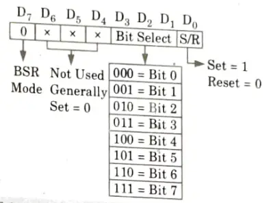
B. Bit Set-Reset (BSR) Mode:
- 1. By sending an OUT command to the control register, any one of the eight bits on port C can be set or reset in this mode.
- 2. This functionality can be utilized to set or reset certain bits as if they were output ports while port C is being used for control/status operation.
d. Analyze the PSW of 8051 and also explain the relevant flag bits.
Ans. PSW: A register with 8 bits is called the Program Status Word (PSW) register. The flag register is another name for it. The PSW register is 8 bits wide, however the 8051 only uses 6 of those bits. User-definable flags are the two unused bits.
In this, four flags are called conditional flags, meaning that they indicate some conditions that result after an instruction executed:
CY, the carry flag: This flag is set whenever there is a carry out from the D7 bit. This flag bit is affected after an 8-bit addition or subtraction. It can also be set to 1 or 0 directly by an instruction such as “SETB C” and “CLR C” where “SETB C” stands for “set bit carry” and “CLR C” stands for “clear carry”.
AC, the auxiliary carry flag: If there is a carry from D3 to D4 during an ADD or SUB operation, this bit is set, otherwise, it is cleared. This flag is used by instructions that perform BCD (binary coded decimal) arithmetic.
P, the parity flag: The parity flag reflects the number of is in the A (accumulator) register only. If the A register contains an odd number of 1s, then P= 1. Therefore, P= 0 if A has an even number of 1s.
Ov, the overflow flag: When the outcome of a signed number operation is too large and the high-order bit overflows into the sign bit, this flag is set. The carry flag is typically used to identify mistakes in unsigned arithmetic operations. Only signed arithmetic errors are detected using the overflow flag.
e. Discuss the significance of I/O ports along-with their dual roles in 8051.
Ans. There are four I/O ports in 8051 microcontroller:
- i. Port 0: Eight pins are used by Port 0 in total (pins 32-39). It is applicable to both input and output. Each pin of port 0 needs to be externally linked to a 10 k pull-up resistor in order to be used as both input and output ports.
- ii. Port 1: Eight pins are used by Port 1 in total (pins 1 through 8). It has input and output capabilities. Unlike port 0, which requires pull-up resistors, this port already includes internal pull-up resistors. Port l is set up as an input port after a reset.
- iii. Port 2: Eight pins are used by Port 2 in total (pins 21 through 28). It has input and output capabilities. As Port 2 already contains internal pull-up resistors, no additional resistors are required. Port 2 is set up as an input port after a reset.
- iv. Port 3:
- 1. Port 3 uses 8 pins in total (pins 10 through 17). It has input and output capabilities. Like P1 and P2, P3 does not require any pull-up resistors.
- 2. Although though port 3 is initially set up as an input port, this is not how it is most frequently utilised. Moreover, port 3 has the ability to deliver some crucial signals from outside, such interrupts.
Section 3: Aktu Notes Pdf of Microprocessor and Microcontroller
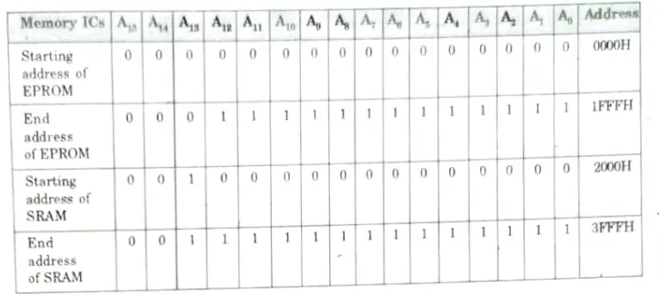
a. Interface EPROM of 16 Kusing 8K x 8 chips and a RAM of 8K using 4K x8 chips to the system lines of 8085 using a 3×8 decoder.
Ans. 1. Fig. shows the desired memory system using IC 2764 (8K) EPROM and 6264 (8K) SRAM memory requires 13 address lines (A0 – A12) since 213 = 8K.
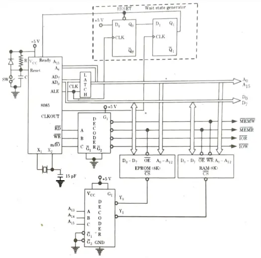
2. The remaining address lines (Aj3-A15) are decoded to generate chip select CS(bar) signals. IC 74LS138 is used as decoder.
3. When (A15 – A13) address lines are zero, the Y0 output of decoder goes low and selects the EPROM.
4. This means that A15 – A13 address lines must be zero to read data from EPROM. The address lines A0 – A12 Select the particular memory location in the EPROM when A15 – A13 lines are zero.
5. Similarly when addresslines A15 -A13 are 001, the Y1 output of decoder goes low and selects the RAM.
Table. Memory map
b. Demonstrate the interfacing of output and input devices with 8085 along-with a suitable diagram. Also explain the relevant instructions used.
Ans. A. Interfacing of output devices:
1. A seven segment display is an output device made up of seven segments of light emitting diodes and one segment for the decimal point.
2. Fig. depicts the physical configuration of these LEDs.
3. To show a number, the required segments are lit by sending the proper signal to cause current to flow through the diodes.
4. Common cathode and common anode are the two groups into which seven segment LED are divided.
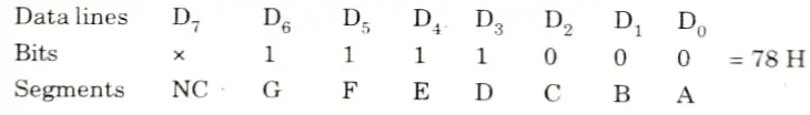
5. The seven segments A to G are connected, accordingly, to data lines D and LP. If a decimal point is utilized, data line D is attached to DP.
6. The kind of seven segment LED, how the data lines are connected, and the logic needed to light the segment all affect the binary code needed to display a digit.
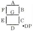
7. Consider a seven segment LED that is connected using 3:8 decoder. The circuit diagram is shown in Fig.
8. Now if we want to display digit 7 on the LED then in common anode seven segment LED, logic 0 is required to be turn ON the segment. The binary code should be equal to 78H.
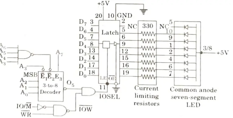
8. Now if we have to design an output port with port address F5 H, then address line should have following logic.
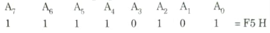
9. This can be achieved using A2, A1 and A0 as input lines to the decoder. A1 can be connected to active low enable E, and the remaining address E2(bar) lines can be connected to E2(bar) through 4-input NAND gate. Fig. shows the output port with address F5 H.
B. Interfacing of input devices:
1. Interfacing of input device is similar to that of output device except that there is difference in bus signals and circuit components.
2. Consider an eight DIP switches interfaced using 3:8 decoder. The circuit used for interfacing eight DIP switches is shown in Fig.
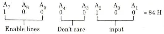
3. The 3 : 8 decoder is used to decode low order bus and tri-state buffer is used to interface the switches with data bus. The port can be accessed with address 84 H however it has multiple address.
4. The device has two groups of four buffers each and they are controlled by active low signals OE(bar).
5. When OE(bar) is low the input data shown up on the output lines and when OE(bar) signal is high, the output lines assumes high impedance state.
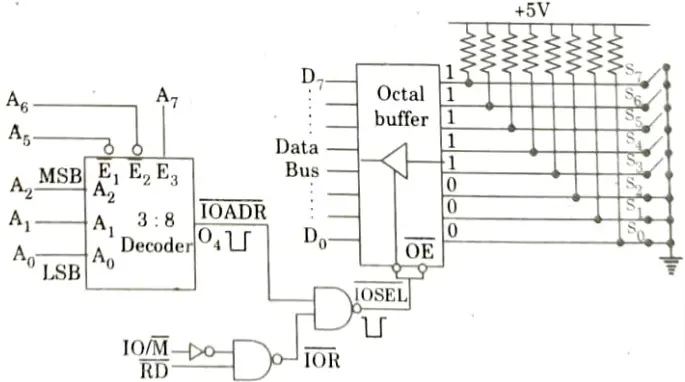
6. The low order address bus, except the lines A4 and A3 is connected to the decoder. The address lines A3 and A4 are left in don’t care state.
7. The output line O4 of the decoder goes low when the address bus has following address
8. The control signal I/OR(bar) is generated by ANDing the IO/M(bar) and RD(bar) in a negative NAND gate, and the I/O select pulse is generated by ANDing the output of decoder and control signal IOR(bar)
9. When the address is 84 H and control signal IOR(bar) is asserted, the I/O select the pulse enable tri-state buffer and logic levels of the switches are placed on data bus. The 8085 then begins to read switch position and places the reading in accumulator.
Section 4: Microprocessor and Microcontroller Aktu Quantum Notes Pdf
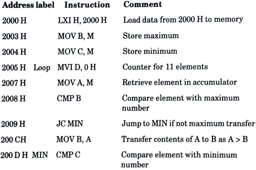
a. Write an assembly language program to find the largest number in a series of number stored from location 2000 H to 200 AH. Store the result at location 3000 H. Explain the program with a relevant flowchart.
Ans.

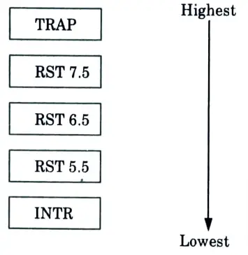
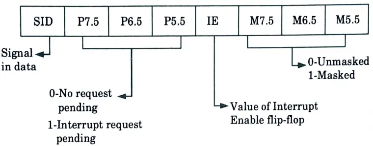
b. Discuss the priorities of the interrupts available in 8085. Give a detailed explanation of SIM and RIM.
Ans. A. Priority of interrupts:
- 1. A microprocessor will carry out an interrupt service request (ISR) in accordance with the priority of the interrupts when it receives multiple interrupt requests at once.
- 2. The priority of interrupts is shown in Fig.
B. SIM (Set Interrupt Mask):
- 1. It is used to implement the hardware interrupts (RST 7.5, 6.5, and 5.5) by setting different bits to create masks or produce output data via the Serial Output Data (SOD) line.
- 2. First the required value is loaded in accumulator then SIM will take the bit pattern from it.
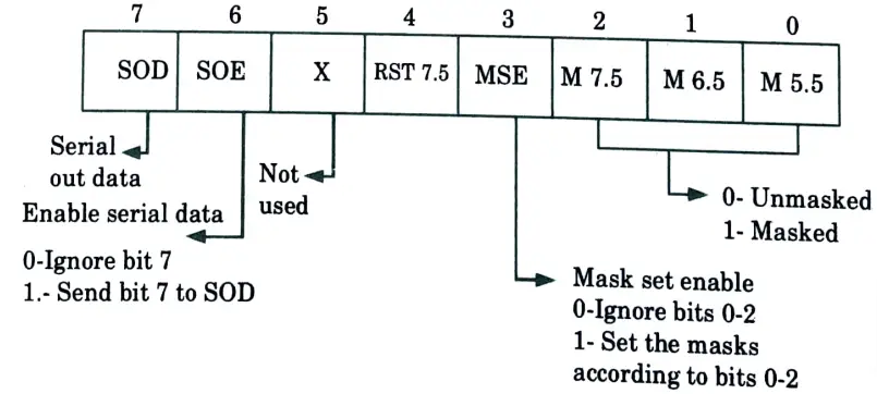
C. RIM (Read Interrupt Mask):
- 1. This instruction is used to read the status of the hardware interrupts (RST 7.5, RST 6.5, RST 5.5) by loading into the A register a byte which defines the condition of the mask bits for the interrupts.
- 2. It also read the condition of SID (Serial Input Data) bit on microprocessor.
Section 5: Microprocessor and Microcontroller Aktu Important Repeated Questions
a. Discuss the various addressing modes available in 8086 along-with examples.
Ans. The addressing modes for sequential control transfer instructions are explained as follows:
- 1. Immediate addressing mode: Immediate data is a component of the instruction in this sort of addressing method and takes the shape of subsequent bytes.
- Example: MOV AX, 0005 H
- 2. Direct addressing mode: In this mode, a 16-bit memory address (offset) is directly specified in the instruction as a part of it.
- Example: MOV AX, [5000 H]
- 3. Register addressing mode: In this approach, the information is kept in a register and referred to by that specific registration. Except for IP, all registers are usable in this mode.
- Example: MOV BX, AX.
- 4. Register indirect addressing mode:
- i. The offset registers are used to indirectly determine the address of the memory region that contains the data or operand. The term “register indirect mode” refers to this addressing technique.
- ii. In this mode, the offset address of data is in either BX or SI or DI registers. The default segment is either DS or ES.
- Example: MOV AX, [BX]
- 5. Indexed addressing mode: The offset of the operand is kept in one of the index registers in this addressing style. The default segments for index registers SI and DI are DS and ES, respectively. The register indirect addressing mode is a specific case of this approach.
- Example: MOV AX, [SI]
- 6. Register relative addressing mode: In this addressing method, the data is accessible at a valid address created by combining the contents of any one of the default segment’s registers BX, SI, or DI with an 8-bit or 16-bit displacement (ES or DS).
- Example: MOV AX, 50 H[BX]
- 7. Based indexed addressing mode: In this addressing mode, the content of an index register is added to the content of a base register (BX or BP) to provide the effective address of the data (SI or DI). Either ES or DS could be the default segment register.
- Example: MOV AX, [BX] [SI];
- 8. Relative based indexed addressing mode: The sum of the contents of any one of the base registers (BX or BP) and any one of the index registers in a default segment is added to an 8-bit or 16-bit displacement to create the effective address.
- Example: MOV AX, 50 H[BX][SI]
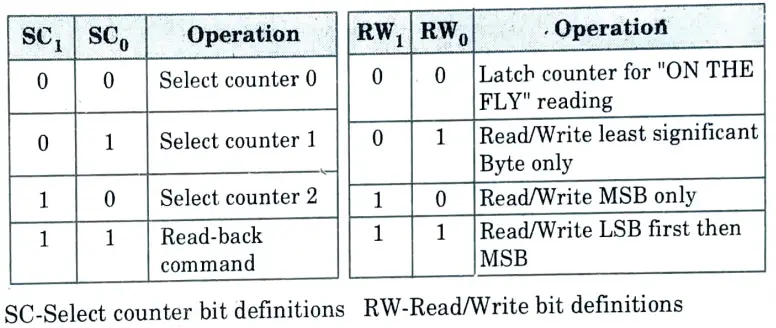
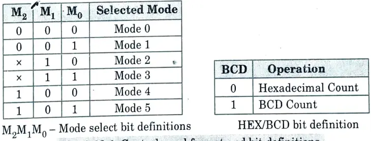
b. Demonstrate the architecture of 8253/54 programmable timer and discuss the control word register.
Ans. A. Architecture of 8253/54 programmable timer:
- 1. Fig. displays the internal block diagram of 8253. Three separate 16-bit counters are present in the programmable timer device 8253. Hence, three independent delays or three independent counters can be generated concurrently.
- 2. The three internal command word registers are programmed to operate the three countérs.
- 3. The 8253’s internal circuit is interfaced to the bus of microprocessor systems by an 8-bit, bi-directional data buffer.
- 4. When an IN or OUT instruction is executed, data is sent or received by the buffer. Whereas the OUT instruction writes data to a peripheral, the IN instruction reads data.
- 5. The three counters offered in 8253 are identical in terms of organization but operate independently of one another.
- 6. The specialty of the 8253 counters is that they can be easily read on line . without disturbing the clock input to the counter
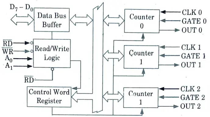
- 7. A0, A1 pins are address input pins and are required internally for addressing the control word registers and the three counter registers.
- 8. A low on CS(bar) line enables the 8253. No operation will be performed by 8253 till it is enabled.
B. Control word register:
- 1. Any of the 8253’s six operational modes can be used. To determine the operation mode of each of the 8253 counters, a control word must be written to initialize each counter.
- 2. All of the counters have the option of operating in any of the modes, or even in multiple modes simultaneously.
- 3. The control word format is shown Fig. along with the definition of each bit:
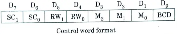
- 4. It should be noted that when writing a count into a counter, the count is only entered once the data has been transferred to the data bus and a falling edge has since appeared at the peripheral’s clock pin.
- 5. Before the falling edge occurs, reading the counter may result in trash data.
Section 6: Aktu Quantum Notes Pdf of Microprocessor and Microcontroller
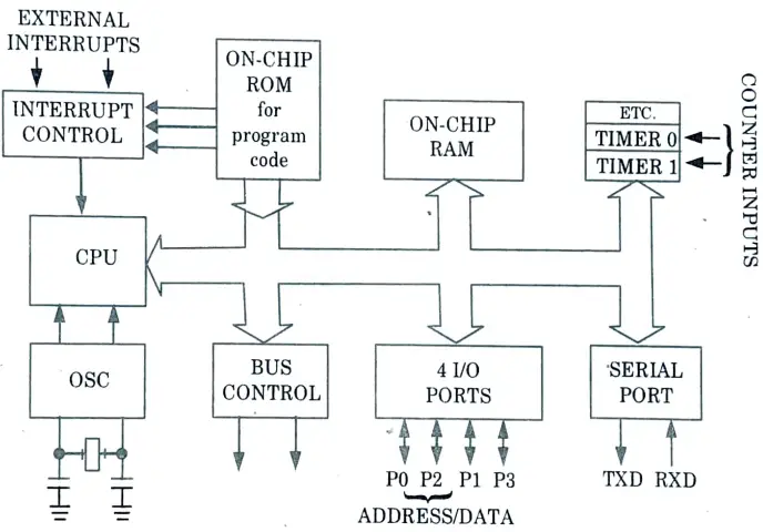
a. Analyze the architecture of 8051 microcontroller along-with a suitable block diagram.
Ans. Architecture of 8051 microcontroller :
- 1. The 8051 microcontroller is a single-chip device that includes 128 bytes of RAM, 4 Kbytes of on-chip ROM, two timers, a serial port, and four ports, each 8 bits wide. Another name for it is “system on a chip.”
- 2. The 8051 is an 8-bit processor, meaning that the CPU can work on only 8-bits of data at time. Data larger than 8 bits has to be broken into 8-bit pieces to be processed by the CPU.
- 3. The 8051 has a total of four I/O ports, each 8 bits wide as shown in Fig.
b. Illustrate the addressing modes of 8051 microcontroller. Support your answer with suitable examples.
Ans. A. Addressing mode:
1. The CPU has a variety of ways to access data. The information could be delivered as an immediate value, be stored in memory, or be in a register. Hence, addressing modalities refers to the many methods of accessing the data.
B. Types of addressing mode:
i. Immediate addressing mode:
- 1. The source operand in this mode is constant. As the name suggests, the operand follows the opcode immediately in the assembly of the instruction.
- 2. Information can be loaded into any register, including DPTR, using this mode.
- 3. Here immediate data must be preceded by the pound sign “#”.
Examples:

ii. Register addressing mode:
- 1. This mode involves the use of registers to hold the data to be manipulated.
- 2. Here the source and destination registers must match in size.
Example:

iii. Direct addressing mode:
- 1. Access to internal data memory, including the Special Function Register, is made possible through the direct addressing method (SFR). With direct addressing, an instruction includes an 8-bit internal data memory address that can only be provided in the range of 00 H to FF H.
- 2. In this addressing mode, data is obtained directly from the memory.
Example:
iv. Indirect addressing mode:
- 1. In the indirect addressing method, the actual address that will be utilized to transport data is stored in a register. The only registers that can be utilized as data pointers are registers R0, R1, and DPTR.
- 2. SFR registers cannot be referred to via indirect addressing. While DPTR can carry 16 bit addresses, RO and Rl can each hold 8 bit addresses.
Example:
location whose address is held by R1.
v. Indexed addressing mode:
- 1. With indexed addressing, the base address is kept in a different register (either the programme counter (PC) or the data pointer (DTPR)), while the offset address is kept in the A register.
- 2. The effective address is created by multiplying the value of the base address by the value of the offset address.
- 3. Indexed addressing is used with JMP or MOVC instructions. Look up tables are easily implemented with the help of index addressing.
Example:

Section 7: Important Aktu Repeated Questions of Microprocessor and Microcontroller
a. Discuss the interrupts of 8051. Also give a detailed description of IE and IP registers.
Ans. A. Interrupts of 8081: The six interrupts in the 8051 shown in Table
| S. No. | Interrupt | ROM Location (Hex) | Pin |
| 1. | Reset | 0000 | 9 |
| 2. | External hardware interrupt 0 (INTO) | 0003 | P3.2(12) |
| 3. | Timer 0 interrupt (TF0) | 000B | |
| 4. | External hardware interrupt 1 (INT1) | 0013 | P3.3(13) |
| 5. | Timer 1 interrupt (TF1) | 001B | |
| 6. | Serial COM interrupt (RI and TI) | 0023 |
- 1. Reset : When the reset pin is activated, the 8051 jumps to address location 0000.
- 2. The timers will each have two interrupts: one for timer 0 and one for timer 1. The interrupt vector table’s memory addresses 000BH and 001BH, which correspond to timers 0 and 1, respectively.
- 3. Two interrupts are set aside for hardware external hardware interrupts. Pin numbers 12 (P3.2) and 13(P3.3) in port 3 are for the external hardware interrupts INTO and INT1 respectively. These external interrupts are also referred to as EX1 and EX2.
- 4. Serial communication has a single interrupt that belongs to both receive and transmit. The interrupt vector table location 0023H belongs to this interrupt.
B. IE (Interrupt Enable) Register:
- 1. This register is responsible for enabling and disabling the interrupt.
- 2. EA register is set to one for enabling interrupts and set to 0 for disabling the interrupts.
- 3. Its bit sequence and their meanings are shown in table.
Table IE (interrupt enable) register
| Bit | Symbol | Description |
| IE.7 | EA | Enable/disable |
| IE.6 | – | Undefined |
| IE.5 | ET2 | Enable timer 2 interrupt (8051) |
| IE.4 | ES | Enable serial port interrupt |
| IE.3 | ET1 | Enable timer 1 interrupt |
| IE.2 | EX1 | Enable external 1 interrupt |
| IE.1 | ET0 | Enable timer 0 interrupt |
| IE.0 | EX0 | Enable external 0 interrupt |
C. IP (Interrupt Priority) register of 8051: We can change the priority levels of the interrupts by changing the corresponding bit in the Interrupt Priority (IP) register as shown in the following table.
Table IP (interrupt priority) register
| Bit | Symbol | Description |
| IP.7 | – | Undefined |
| IP.6 | – | Undefined |
| IP.5 | PT2 | Priority for timer 2 interrupt (8051) |
| IP.4 | PS | Priority for serial port interrupt |
| IP.3 | PT1 | Priority for timer 1 interrupt |
| IP.2 | PX1 | Priority for external 1 interrupt |
| IP.1 | PR0 | Priority for timer 0 interrupt |
| IP.0 | PX0 | Priority for external 0 interrupt |
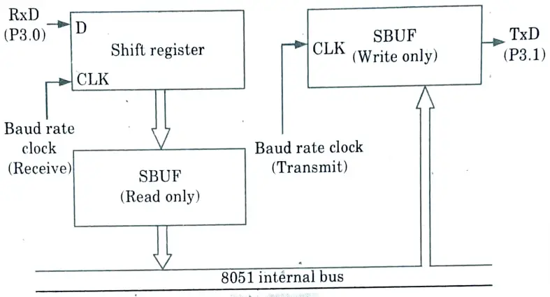
b. Analyze the process of serial communication in 8051 and also discuss the relevant Special Function Registers (SFR’s) used in serial communication.
Ans.
- 1. The 8051’s serial port is full duplex, which allows for simultaneous transmission and reception. It stores data in register SBUF. Data transmission is governed by register SCON, data rates by register PCON, and data transfer via pins RxD (P3.0) and TxD (P3.1).
- 2. On the 8051, SBUF is an 8-bit register reserved for serial communication. It may be found at 99 H. It can be addressed in 8051 just like any other register.
- 3. Reading SBUF allows access to received data, while writing to SBUF loads data for transmission.
- 4. There are two separate and distinct register, the transmit write-only register, and the receive read-only register. This is shown in Fig.
- 5. The way in which SBUF is used for the transmission and reception of the data during serial communication is explained below:
- a. Transmission: When a byte of data is to be transmitted via the TxD pin, the SBUF is loaded with this data byte. As soon as a data byte is written into SBUF, it is framed with the start and stop bits and transmitted serially via the TxD pin.
- b. Reception: The 8051 deframes data that it receives serially on its RxD pin. A byte of data is divided into the start and finish bits. This kind is registered in the SBUF.
6 thoughts on “Microprocessor and Microcontroller Aktu Question Paper 22-23, Notes Quantum Pdf,”