Discover thorough notes on Digital Electronics and Computer Organisation from BCA solved exam papers. To succeed in your studies, reveal the fundamentals of digital circuits and computer architecture.
Dudes 🤔.. You want more useful details regarding this subject. Please keep in mind this as well.

Important Questions For Digital Electronics and Computer Organisation:
* Important Short Questions
* Solved Question Paper
* Syllabus
Section A: Digital Electronics and Computer Organisation Very Short Question Answers
Q1. Write De Morgan’s Law.
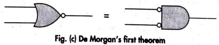
Ans. Fig. (a, i) shows an inverter on the output line of an OR gate. The logic circuit is drawn in the abbreviated form shown in Fig. (a, ii), which can be referred to as NOR gate. Its Boolean equation is :
Y = (A + B)’ …..(i)
We can read the Eq. (i) as ‘Y equals NOT A OR B’ or ‘Y equals the complement of A OR B’. The only way to get a high output is to have both inputs low, as shown in Table 1.
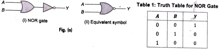
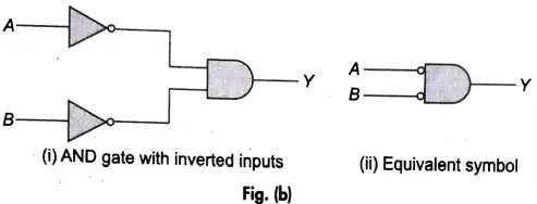
Fig. (b, i) shows inverters on the input lines of an AND gate. The logic circuit is drawn in the abbreviated form shown in Fig. (b, ii), which can be referred to as bubbled AND gate. Its Boolean equation is:
Y = A’ B’ ……(ii)
The only way to get a high output is to have both inputs low, as shown in Table 2.
Notice that both the truth tables (shown in table 1 and table 2) are identical. It means a NOR gate produces the same output as a bubbled AND gate. In other words, the circuits are interchangeable, i.e. given any logic circuit with NOR gates, you can replace each NOR gate by a bubbled AND gate. Similarly, given any logic circuit with bubbled AND gates, you can replace each bubbled AND gate by a NOR gate.
Since, the outputs are equal for the same inputs, we can equate the right-hand members of
Eq. (i) and Eq. (ii) to get:
(A + B)’= A’ B’ ……(iii)
This identity is known as De Morgan’s first theorem, which says that the complement of a sum equals the product of the complements. Fig. (c) is the graphical meaning of De Morgan’s first theorem. Visualise the right-hand member of Eq. (ii) as the output of a bubbled AND gate; and the left-hand member of Eq. (iii) as the output of a NOR gate. That means, a NOR gate is equivalent to a bubbled AND gate.
Q2. Differentiate between flip flop and latches.
Ans. Difference between Flip-Flops and Latches
| S.No. | Flip-Flop | Latch |
| 1. | Flip-flop is a bistable device, i.e. It has two stable states that are represented as 0 and 1. | Latch is also a bistable device whose states are also represented as 0 and 1. |
| 2. | It checks the inputs but changes the output only at times defined by the clock signal or any other control signal. | It checks the inputs contínuously and responds to the changes in inputs immediately |
| 3. | It is a edge triggered device. | It is a level triggered device. |
| 4. | Gates like NOR, NOT, AND, NAND are building blocks of flip-flops. | These are also made up of gates. |
| 5. | They are classified into asynchronous or synchronous flip-flops. | There is no such classification in latches. |
| 6. | It forms the building blocks of many sequential circuits like counters. | These can be used for the designing of sequential circuits but are not generally preferred. |
| 7. | A flip-flop always have a clock signal. | Latch does not have a clock signal. |
| 8. | Flip-flop can be build from latches. | Latches can’t build from gates. |
| 9. | Examples: D flip-flop and JK flip-flop. | Examples: SR latch and D latch. |
Q3. Differentiate between combinational logic circuit and sequential circuits.
Ans. Difference between Combinational and Sequentlal Circuits
| S.No. | Basis of difference | Combinational circuit | Sequential circuit |
| 1. | Definítion | A combinational circuit is a sort of circuit in which the output is independent of time and solely depends on the input present at the time. | A sequential circuit, on the other hand, is a sort of circuit in which the output is dependent not only on the current input but also on the prior output. |
| 2. | Feedback | In this circuit output does not depend on the time instant. no feedback is required for its next output generation. | The circuit’s output is dependent on its prior feedback, so the output from the previous input is used as feedback when creating the subsequent output generation. |
| 3. | Performance | Combinatorial circuits function faster and more effectively than sequential circuits since they just require the input of current instant. | Comparatively slower and with poorer performance than combinational circuits are sequential circuits. |
| 4. | Complexity | No implementation of feedback makes the combinational circuit less complex. | Implementation of feedback makes sequential circuit more complex. |
| 5. | Elementary blocks | Elementary building blocks for this circuit are logic gates. | Building blocks for sequential circuit are flip-flops. |
| 6. | Operation | Combinational circuits are mainly used for arithmetic as well as Boolean operations. | Sequential círcuits are mainly used for storing data. |
Q4. Construct half subtractor using logic gates.
Ans. Construction of half subtractor using logic gates:
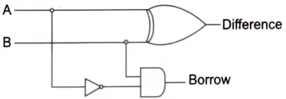
The circuit of the half subtractor can be built with two logic gates namely NAND and EX-OR gates. This circuit gives two elements such as the difference as well as they borrow.
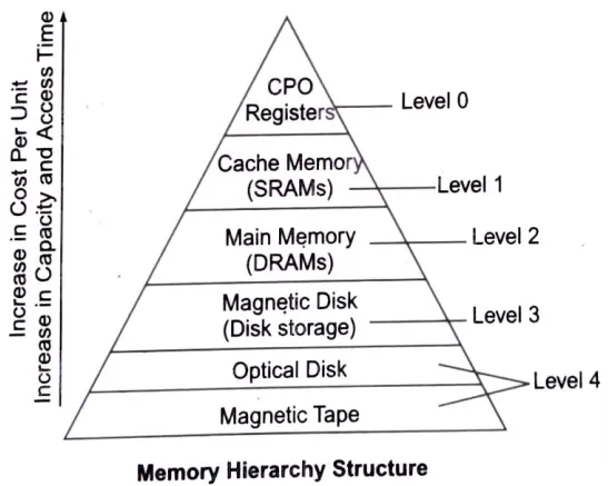
Q5. Draw the memory hierarchy structure and mark the arrow from low to high (speed) and high to low (Cost).
Ans. Memory hierarchy structure is an improvement to memory organisation in computer system design that reduces access time. The faithfulness of references behaviour of a programme served as the foundation for the creation of the memory hierarchy. The different levels of memory hierarchy are clearly shown in the diagram below.
Section B: Digital Electronics and Computer Organisation Short Question Answers
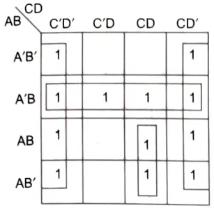
Q6. Minimise the following Boolean function using K-map.
F(A, B, C, D) = Σ (3, 4, 5,7,9, 13, 14, 15)
Sol. Figure given below shows the K-map for the given Boolean function:
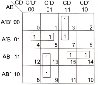
There are four pairs in third column, second row, third row and second column namely:
A ‘CD’, A ‘BC’
ABC and ACD respectively.
Thus, the simplified function in sum of products form is:
F = A’ CD + A ‘BC’ + A C’D + ABC
= (AC + AC) D + B (AC + AC)
= {AC + (AC)} D + {AC + (AC)’} B
= D + B
Q7. (i) Convert the SR flip flop to JK flip flop draw the truth table of JK flip flop also.
Ans. RS (or SR) Flip-Flop : Fig. (a) shows the graphic symbol of the RS flip-flop. This flip-flop has three inputs: S (for st), R (for reset) and C (for clock-pulse). It has one output: Q Sometimes, this flip-flop may also have a complemented output, which is indicated with a small circle at the other output terminal:
Table 1 shows the characteristic table of the operation of the RS flip-flop. Here, Sand R columns give the binary values of the two inputs. QC) represents the present state and Q(t +1) represents the next state :
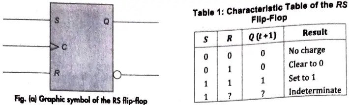
The operation of the RS flip-flop is as follows: If there is no signal at C, the output of the flip-flop cannot change irrespective of the values of S and R. Whenever, C changes from 0 to 1, the output of the flip-flop will change according to the values ofS and R. IfS = R= 0, a clock transition produces no change of state, that is, 0(t + 1) = Q(t). If S = 0 and R=1, the flip-flop goes to clear state, i.e. 0. If S = 1 and R = 0, the flip-fon goes to set state, i.e. 1.
When S = R =1, SR flip-flop produces an indeterminate next state. This condition makes this flip-flop difficult to manage and therefore it is seldom used in practice.
JK Flip-Flop: Fig. (c) shows the graphic symbol of the )K flip-flop. Similar to SR flip-flop, theJA flip-flop has three inputs: J (for set), K (for reset) and C (for clock-pulse). It has one output: Q Sometimes, this flip-flop may also hayes complemented output, which is indicated with a small circle at the other output terminal :
Table 3 shows the characteristic table of the operation of the JK flip-flop. Here, J and K columns give the binary values of the two inputs. Q(t) represents the present state and Q(t + 1) represents the next state.
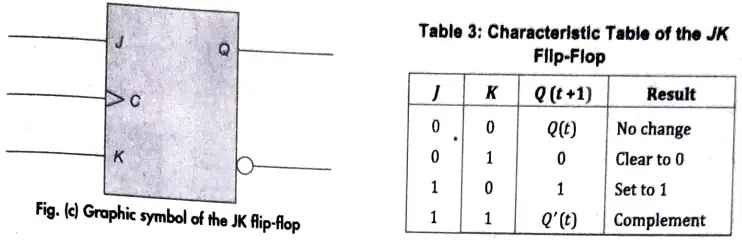
The operation of the JK flip-flop is as follows: If there is no signal at C, the output of the filip-flop cannot change irrespective of the values of I and K. Whenever, C changes from 0 to 1, the output of the flip-flop will change according to the values of J and K. If J = K = 0, a cock transition produces no change of state, i.e. Q(t + 1) = 0 (t). IfJ= 0 and K= 1, the flip-flop goes to clear state, i.e. 0. If J = 1 and K = 0 the flip-flop goes to set state, i.e. 1.
Unlike SR flip-flop, whenJ = K=1, a clock transition switches the outputs of the JK îlip-flop to their complement state; i.e. Q (t + 1) = Q’(t). Clearly, a JK flip-flop is a refinement of the SR flip-flop in that the indeterminate condition of the SR type is defined in the JK type.
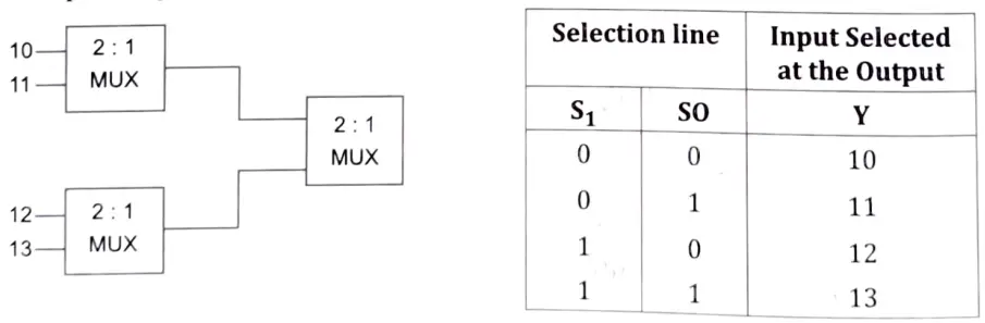
(ii) Implement 4 : 1 multiplexer using 2 : 1 multiplexer.
Sol. Let us take on 4 input MUX. It will have 2 selection lines. On the analogy Boolean expression and its truth table, the input-output will be as follows:
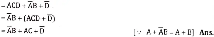
Q8. (i) Simplify the expression:

Sol.
Using Boolean Simplification,
(ii) How many flip flops are needed to implement a 32 bit register?
Sol. In order to prevent a bit from “leaking” away, two or more transistors are connected in a feed-back loop using a flip flop. A flip flop register is an arranged group of flip flops. As an illustration, the majority of modem processors feature a set of 32 or 64 bit on chip registers. 32 flip flops, each storing one bit, make up a 32 bit register.
Section C: Digital Electronics and Computer Organisation Detailed Question Answers
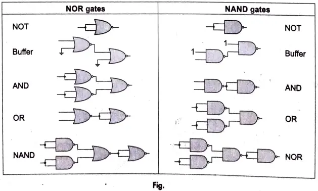
Q9. (i) Which gates are called universal gates and why?
Ans. Universal Gate : The NAND and NOR gates are obtained from basic gates. NAND and NOR gates are also called as universal logic gates. Universal means multipurpose. It is possible to implement any logic expression using only NAND or only NOR gates.
Boolean expression consists of various basic logic operations such as AND, OR and NOT, NAND or NOR gates are used to implement basic logic operations because their fabriçation on ICs is very easy as compared to fabrication of other gates.
Basic gates implementation by using NOR and NAND gate are shown in figure.
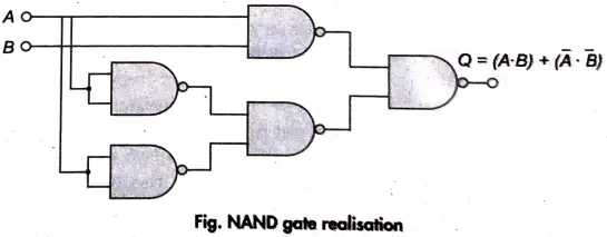
(ii) Draw a full subtractor circuit using NAND gate.
Ans. Implementation of its Circuit using NAND Gates : Electronic circuits like adders, subtractors, parity checkers, etc. that conduct arithmetic operations and data checking are the major applications for XNOR gates. Digital comparator circuits use XNOR gates because they may be used to compare the magnitude of two binary digits or integers since they produce a logic level 1 output when their two inputs are equal.
Q10. What do you mean by shift register? What is the need of shift register? Draw and explain bidirectional shift register.
Ans. Shíft Register : It is direct application of flip-flops. A register capable of shifting its binary information either to the right or to the left is called a shift register.
Serial shift register consists of a chain of fip-flops in which the output of one flip-flop is connected to the input of the next flip-flop. All flip-flops receive a common clock-pulse which causes the shift from one stage to the next stage.
A 4-bit serial shift register using the D flip-flops is shown in given figure :
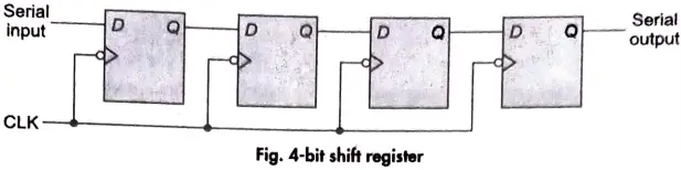
A 4-bit serial shift register utilising D flip-flops. The D input of the following flip-flop is connected to the output of the previous flip-flop on its right side. The contents of the register are shifted one bit to the right with each clock-pulse (-ve edge trigger). What enters the leftmost flip-flop during the shift is determined by the serial input. Before applying a pulse, the serial output is collected from the right-most flip-flop’s output. As a result, register move its contents to the right. The contents of the register move to the left if the page is turned upside down. As a result, a unidirectional shifts register can be used as either a shift-right or shift-left register.
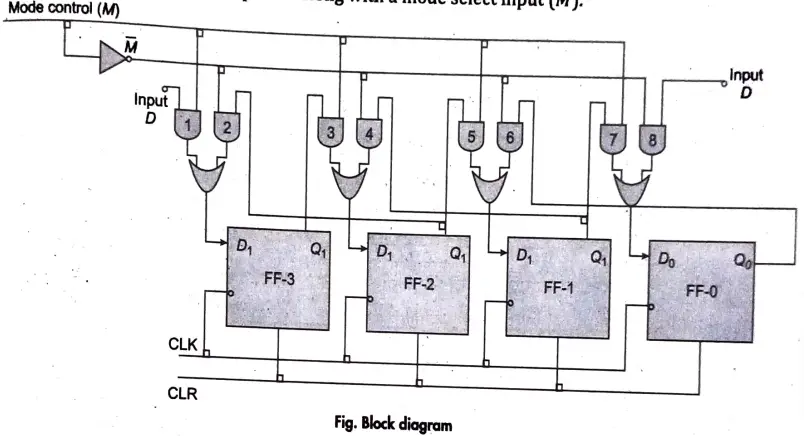
Bi-directional Shift Register : If a binary number is shifted left by one position, then it is equivalent to multiplying the original number by 2. Similarly, if a binary number is shifted right by one position, then it is equivalent to dividing the original number by 2. Hence, if we want to use the shift register to multiply and divide the given binary number, then we should be able to move the data in either left or right direction. Such a register is called bi-directional register. A four bit bi-directional shift register is shown in figure. There are two serial inputs namely the serial right shift data input DR, and the serial left shift data input DL along with a mode select input (MJ).
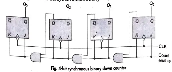
Q11. Draw and explain 4-bit binary synchronous counter.
Ans. The logic diagram of 4-bit synchronous binary down counter is shown in given figure :
Q12. (i) Differentiate between EPROM and EEPROM.
Ans.
| S. No. | EPROM | EEPROM |
| 1. | EPROM is a programmable ROM that can be erased and reused. | EEPROM is a user modifiable ROM that can be erased and reprogrammed repeatedly through a normal electrical voltage. |
| 2. | EPROM stands for Erasable Programmable Read Only Memory. | EEPROM stands for Electrically Erasable Programmable Read Only Memory. |
| 3. | We can reprogram EPROM using ultraviolet light. | We can reprogram EEPROM using electrical charge. |
(ii) Differentiate between SRAM and DRAM.
Ans. Difference between Dynamic RAM and Static RAM
| S. No. | Basis of difference | Dynamic Random Access Memory (DRAM) | Static Random Access Memory (SRAM) |
| 1. | Memory cells | DXAM Contains more memory cells per unit area. | SRAM contains less memory cells per unit area as compared to DRAM. |
| 2. | Access time | Its access time is greater than that of static RAMs. | It has less access time and hence are faster memories. |
| 3. | Contents | Dynamic RAM stores the data as charge on the capacitor. It consists of MOSFET and the capacitor for each cell. | Static RAM consists of a number of flip-flops. |
| 4. | Lifetime of change | The information stored in dynamic RAM gradually disappears as the charge on the capacitors decreases. | The information stored in static RAM does not decrease with time as it does not have any capacitors. |
| 5. | Refreshing circuitry | Refreshing circuitry is required for maintaining the charge on the capacitors after every few milliseconds. | Refreshing circuitry is not required. |
| 6. | Cost factor | DRAMs are cheap. | SRAMs are expensive. |
(iii) Differentiate between L1 cache and L2 cache
Ans. Differences between L1 and L2 Cache
Although both L1 and L2 are cache memories they have their key differences L1 and L2 are the first and second cache in the hierarchy of cache levels L1 has a smaller memory capacity than L2. Also L1 can be accessed faster than L2. L2 is assessed only if the requested data in not found in L1.L1 is usually in built to the chip, while L2 is soldered on the motherboard very close to chip. Therefore L1 has very little delay compared to L2. Because L1 is implemented using SRAM and L2 is implemented using DRAM.
13. (i) Differentiate between ROM and PROM.
Ans. The difference between ROM and PROM are as follows:
- (a) ROM stands for read memory. While PROM stands for programmable read-only memory.
- (b) ROM refers to a memory chip storing permanent data and instruction, while in PROM is the type of read-only memory. It is a type of memory that can only be modified once not again and again.
- (c) ROM cannot be erased or written too. Memory chips that are programmed in factories for large run production. PROM is progammed only once by blown of internal fuses permanently and is also called field programmable ROM and is programmed by using a ROM programmer in the lab or onsIte.
- (d) ROM is non volatile, which means it contents are not lost when power is removed from the computer. Most of the ROM chips are designed to be modified so, there are less chance of any type of error. User can modify it by using EPROM and EEPROM.
(ii) Describe USB.
Ans. A host controller, such as a personal computer or smartphone, and devices can communicate with one another using a common interface called a Universal Serial Bus (USB). It establishes connections between auxiliary devices such external hard drives, flash drives, microphones, keyboards, printers, scanners, and media players.
The purpose of a USB is to improve plug-and-play and support hot swapping. Plug-and-play enables the Operating System (OS) to automatically configure and discover a new peripheral device without the need to restart the computer. Hot swapping additionally enables the removal and replacement of a new peripheral without the need for a reboot.
(iii) Differentiate between primary memory and secondary memory. Also list the examples of primary memory and secondary memory.
Ans. 1. Primary Memory : Primary memory is where the data that is being processed is stored. It is also known as internal storage, working memory, main memory, and primary storage. It has exceptionally high transmission and reception speeds for data. Compared to secondary memory, it has a lesser storage capacity but a faster access time.
A computer system’s core storage is made up of numerous small storage spaces referred to as locations or cells. The word length of that specific memory is the maximum number of bits that can be stored in each of these locations. Each address for a memory word is different. The standard word length in modern computers is 16 or 32 bits.
The computer uses the primary storage to keep track of its commands, data, recently created outcomes of processing, and intermediate results of processing. Information can only be stored in primary storage while the computer system is turned on (RAM, cache memory, etc.). Additionally, primary storage often has a small amount of storage space.
The amount of bytes a computer system can hold is used to define the primary memory capacity. The standard units of measurement are KB (Kilobyte), MB (Megabyte), and GB (Gigabyte). RAM (Random Access Memory) and ROM (Read Only Memory) are two examples of fundamental memories.
2. Secondary Memory : Long-term memory, auxiliary memory backup storage, and secondary storage are other names for secondary memory. It keeps info that isn’t just being used. In the specified medium, the data is permanently stored using this method of storage. It operates at a significantly slower rate than the primary storage. Compared to primary storage, cost per bit is minimal.
The issues with the primary storage are fixed with the secondary storage. Even when the computer system is turned off, the backup storage can keep data. It is typically used to store programme instructions and data that the computer isn’t currently executing but needs to keep for subsequent processing. Large amounts of data can be stored on it because of its unlimited storage capacity.
(iv) Explain the concept of virtual memory.
Ans. Virtual Memory : Between primary memory and secondary memory, virtual memory serves as a cache. In order to have data ready in the main memory when needed, data is pre-fetched from the secondary memory (hard disc) into the main memory. The advantage is that accessing data from a hard disc doesn’t experience the significant access delays. In the secondary memory, pages are created and then transferred to the primary memory. The operating system is in charge of managing the memory resources, whereas the memory management unit in the hardware manages this process.
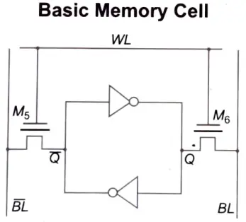
(v) Draw basic cell of memory
Ans.