Microwave and Radar Engineering: AKTU Solved Question Paper provides comprehensive test preparation aids. These answers to the questions aid in conceptual comprehension, problem-solving exercise, and topic selection for the best exam preparation.
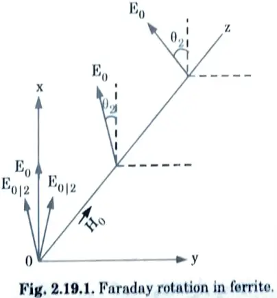
Dudes 🤔.. You want more useful details regarding this subject. Please keep in mind this as well.

Important Questions For Microwave and Radar Engineering:
*Quantum          *B.tech-Syllabus
*Circulars           *B.tech AKTU RESULT
* Btech 4th Year
Section A: Short Question Microwave and Radar Engineering
a. Differentiate dominant and degenerative mode in waveguide.
Ans.
| S. No. | Dominant mode | Degenerative mode |
| 1. | The dominant mode in a waveguide that supports more than one propagation mode is the mode that propagates with the lowest cut-off frequency. | When two or more modes in a waveguide have the same cut-off frequency, they are said to be degenerate modes. |
| 2. | For rectangular TE10 is the dominant mode. | For rectangular waveguide TEmn or TMmn modes for which both m = 0, n ≠ 0 will always be degenerate modes. |
b. Define cut-off wave number (kc). Show that kc2 = ω2 με for lossless dielectric.
Ans. kc is define as the reciprocal of the cut-off wavelength and also can be written as,
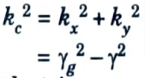
For lossless dielectric
c. Give the difference between isolator and circulator.
Ans.
| S. No. | Isolator | Circulator |
| 1. | It is two port device. | It has multiple port typically 3 or 4. |
| 2. | Isolators are used in optical amplifier and laser to prevent reflections. | Circulators are used to construct optical add drop multiplexer. |
d. What is hybrid ring in microwave ?
Ans. A hybrid ring (also known as a rat race) is a microwave device for combining or dividing microwave power. It is a simple circular design that allows total phase reversal (180° phase shift) of the input microwave signal.
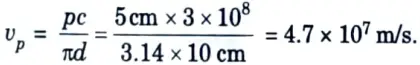
e. In a helical slow wave structure if pitch is 5 cm and diameter is 10 cm, calculate the axial velocity with which wave will propagate.
Ans. Given: p = 5 cm, d = 10 cm
To Find: Axial velocity.
f. What is the condition for sustained oscillation in Reflex Klystron ?
Ans. For oscillations to be sustained, the time taken by the electrons to travel into the repeller space and back to the gap (called transit time) must have an optimum value. In general the optimum transit
g. Explain mode jumping in magnetron ?
Ans. Since the magnetron has eight (or more) coupled cavity resonators, several modes of oscillation are possible. The frequencies of these modes are very close. As a result, magnetron oscillations have a tendency to jump from one mode to another when operating conditions vary slightly. This is known as mode switching.
h. What do you mean by slotted line ?
Ans. One of the fundamental instruments used in radio frequency testing and measurement at microwave frequencies is the slotted line.
i. What is radar clutter ?
Ans. Radar clutter is defined as unwanted backscattered signals or echoes produced by physical objects in the natural environment such as the ground, sea, birds, and so on.
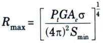
j. Define maximum unambiguous range of radar.
Ans. The maximum range of radar Rmax is the distance beyond which the target cannot be detected. It occurs when the received signal power Pr just equals the minimum detectable signal Smin.
Section B: Long Question of Microwave and Radar Engineering
a. Explain the limitations of conventional active devices at microwave frequency ?
Ans. i. Inter-electrode capacitance :
- 1. Vacuum has a dielectric constant of 1. As the elements of the triodes are made of metal and are separated by a dielectric, capacitance exists between them. This capacitance is inter-electrode capacitance.
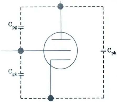
- 2. The capacitance between the plate and grid is Cpg. The grid to cathode capacitance is Cgk. The total capacitance across the tube is Cpk.
- 3. Now, we know that the capacitive reactance is given by
- Xc = 1/2𝛑fC
- 4. So as the input frequency increases, the effective grid to cathode impedance decreases due to decrease in reactance of inter-electrode capacitance.
- 5. At higher frequencies (greater than 100 MHz) it becomes so small that signal is short circuited with the tube. Also, gain of the device reduces significantly.
- 6. This effect can be minimized by taking smaller (reducing the area) electrodes and by increasing distance between them, therefore by increasing reactance.
ii. Lead inductance :
- 1. Lead inductances are effectively in parallel within the device with the inter-electrode capacitance. Inductive reactance is given by:
XL = 2𝛑fL
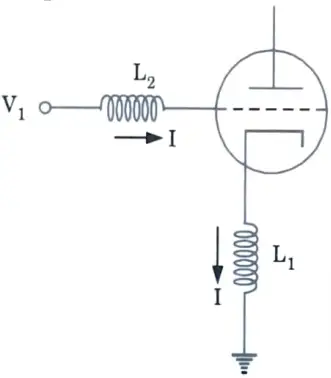
- 2. As the frequency increases, so does the effective reactance of the circuit. This effect raises the device’s frequency limit.
- 3. Cathode lead inductance is shared by grid and plate circuits. This creates a path for degenerative feedback, lowering the circuit’s overall efficiency.
iii. Transit time :
- 1. Transit time is the amount of time electrons take to travel from the cathode to the plate. The transit time is negligible at low frequencies.
- 2. However, at higher frequencies, transit time becomes an appreciable portion of a signal, resulting in a decrease in device efficiency.
iv. Gain bandwidth product :
- 1. The gain bandwidth product is frequency independent. As a result, higher gain for a given tube can only be obtained at the expense of narrower bandwidth.
v. Dielectric loss:
- 1. Dielectric materials are silicon plastic encapsulation materials that are used in microwave devices. The losses caused by these materials are also noticeable at higher frequencies.
b. What is directional coupler? Explain the working principle of 2-hole directional coupler and determine its S-matrix.
Ans. i. Directional coupler :
- 1. The directional coupler has four ports. It is used to sample the energy that passes through the main waveguide.
- 2. They are also used to determine whether a signal passing through two arms is in phase and amplitude.
- 3. There are no reflections at the junction of these four parts. Directional coupler having such property is shown in Fig.
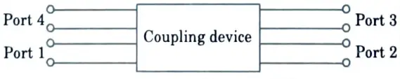
- 4. When the power is incident from port 1 then it is passed to port 2 and port 3, but it does not appears on port 4. Thus port 4 is uncoupled when incident power is fed from port 1.
- 5. Similarly when the power is incident from port 4 then this power is coupled to port 2 and port 3 but not coupled to port 1.
- 6. The directional coupler can also be made from two waveguides. In such cases one waveguide is straight but other is having a curve shape.
- 7. If the power is incident from output end, there should not be any leakage of power into the auxiliary arm. The power incident from output end is called the reverse power.
ii. 2-hole directional coupler: The two holes which are quarter wavelength apart are made between main arm and the auxiliary arm.
Working :
- 1. A two-hole directional coupler is designed to meet the ideal directional coupler requirement of avoiding back power. While travelling between Ports 1 and 2, some power escapes through holes 1 and 2.
- 2. The magnitude of the power depends upon the dimensions of the holes. This leakage power at both the holes are in phase at hole 2, adding up the power contributing to the forward power Pf. However, it is out of phase at hole 1, cancelling each other and preventing the back power to occur.
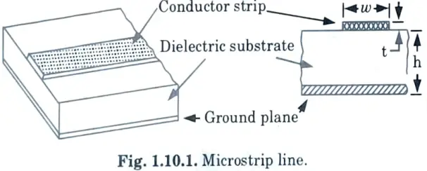
c. What is a Microstrip line ? How does its characteristic impedance change with change in width to height ratio ? Give a reason for using lower dielectric-constant substrate in place of alumina at higher microwave frequencies.
Ans. i. Microstrip line :
- 1. A microstrip line is a skewed strip line. It is a parallel plate transmission line with a dielectric substrate on one face and a thin conducting strip on the other with a width w and thickness t.
- 2. A cover plate is sometimes used for shielding, but it is kept much farther away than the ground plane to avoid interfering with the microstrip field.
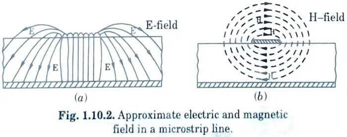
- 3. Because there is no top ground plate or dielectric substrate above the strip, the electric field lines are partially in air and partially in the lower dielectric substrate. As a result, the mode of propagation is not pure TEM, but rather quasi-TEM.
- 4. Due to open structure and any presence of discontinuity, the microstrip line radiates electromagnetic energy.
- 5. The radiation loss is proportional to the square of the frequency.
- 6. The use of thin and high dielectric materials reduces the radiation loss of the open structure where the fields are mostly confined inside the dielectric mode on microstrip lines are only quasi.
8. The pattern for electric field and magnetic field is shown in Fig. 1.10.2.
ii. Characteristic impedance of microstrip line :
1. The characteristic impedance of a microstrip line is determined by the strip-line width, thickness, distance between the line and the ground plane, and the board material’s homogeneous dielectric constant.
2. There are so many methods to calculate characteristic impedance. The well known equation is
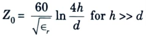
where, ∈re = 0.475 ∈r + 0.67where, ∈r = Relative dielectric constant of the board material.
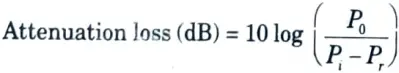
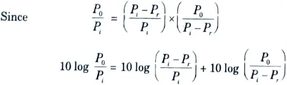
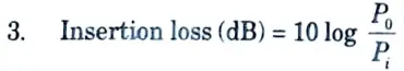
d. What is meant by insertion loss and attenuation? Discuss any one method for measurement of attenuation using microwave test bench.
Ans. A. Attenuation loss :
1. The term attenuation is defined as the ratio in decibels, of either power level or voltage level! between two points in a circuit.
2. When a device or reiwork is inserted in a waveguide, a part of input signal power Pi is reflected from input terminal and remaining part Pi – Pr actually enters the network is attenuated due to non-zero loss of the network.
3. Output signal power P0 is therefore less than input signal power Pi.
B. Insertion loss :
1. Insertion loss is defined as the difference in the power arriving at the terminating load with and without the network in the circuit.
2. Insertion loss = Reflection loss + Attenuation loss
C. Measurement of Attenuation and Insertion loss :
1. For perfect matching Pr = 0 the insertion loss and the attenuation loss will be same.
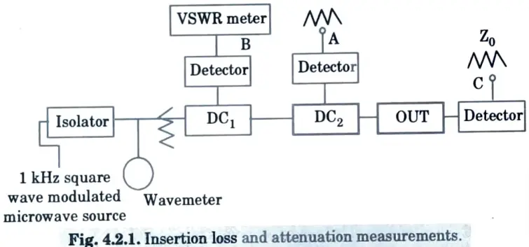
2. Connecting matched load Z0 to port A and C and VSWR meter to port B without disturbing any other setup. The VSWR meter reading gives the ratio Pr / Pi the return loss. The reflection loss 1 – (Pr / Pi) is calculated.
3. Now input attenuator is adjusted to give attenuation equal to the dB coupling of bi-directional coupler.
4. Connecting matched load to port A and B and VSWR meter to port C without disturbing any other setup. The VSWR meter gives the ratio Po / Pi the insertion loss.
5. Attenuation of the network can be determined by subtracting the dB reflection loss from the dB insertion loss.
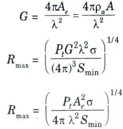
e. Derive the radar range equation.
Ans. 1. If the transmitter power Pt is radiated by an isotropic antenna, the power density is given as :
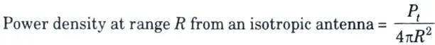
2. The gain of an antenna is a measure of the increased power density radiated in some direction as compared to the power density that would appear in that direction from an isotropic antenna.
3. The maximum gain is defined as :
G = Maximum power density radiated by a directive antenna/power density radiated by a lossless isotropic antenna with the same power input.
4. The power density at the target from a directive antenna with a transmitting gain G is then given by :
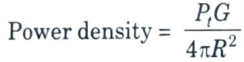
5. The radar cross-section of the target determines the power density returned to the radar for a particular power density incident on the target. It is denoted by σ.

6. The radar captures a portion of the echo energy incident on it. The power received by the radar is given as the product of incident power density times the effective area Ae.
The effective area is related to the physical area and is given as :
Ae = ρa A
where, ρa = antenna aperture efficiency.
7. The received signal power is then given as :
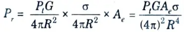
8. The maximum range of a radar (Rmax) is the distance beyond which target cannot be detected. It occurs when Smin = Pr then by rearranging terms, it is given as
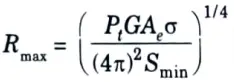
This is the fundamental form of radar range equation.
9. If in case we use the same antenna for both transmitting and receiving, then the relation between the transmit gain G and the receive effective area Ae is given as :
Section 3: Explained Question in Microwave and Radar Engineering
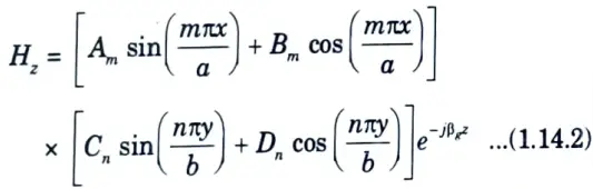
a. Derive the field distribution of TE10 mode in rectangular waveguide. Show that TE01 and TM10 modes do not exist in rectangular waveguide.
Ans. A. Derivation of field distribution of TE10 :
1. It is assumed that waves are propagating in the positive z-direction in the waveguide.
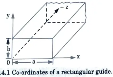
2. Helmholtz equation is ▽2Hz = γ2Hz
3. The TEmn modes in a rectangular guide are characterized by Ez = 0. We know the solution of Helmholtz equation,
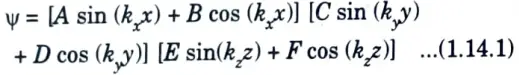
4. Now replacing kx = m𝛑/a and ky = n𝛑/b according to boundary conditions in eg. (1.14.1), we have
5. For a lossless dielectric, Maxwell’s curl equations in frequency domain are
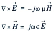
6. In rectangular co-ordinates, their components are
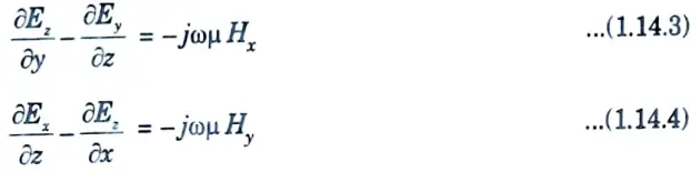
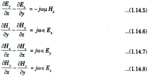
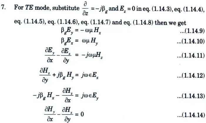
8. On solving eq. (1.14.9), eq. (1.14.10), eq. (1.14.11), eq. (1.14. 12), eq. (1.14.13) and eq. (1.14.14) for Ex, Ey, Hx and Hy in terms of Hz will give the TE mode field equations as
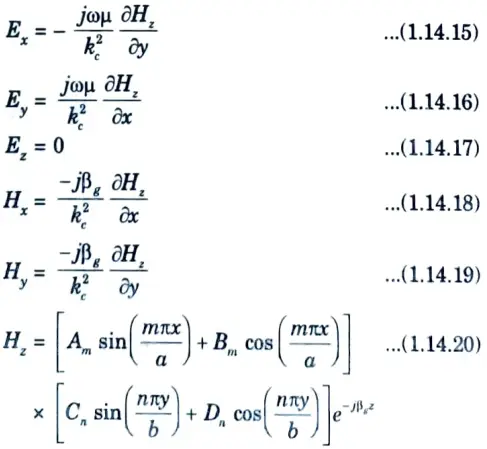
where, kc2 = ω2μ∈ – βg2
9. The normal derivative of Hz must vanish at the conducting surface,
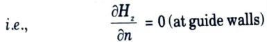
10. Therefore, the magnetic field in positive z-direction becomes
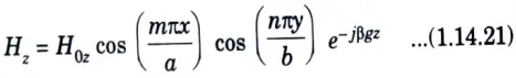
where, H0z = Amplitude constant
11. Substituting eq. (1.14.21) in eg. (1.14.15), eq. (1.14.16), eq. (1.14.18), eq. (1.14.19) and eg. (1.14.20), TEmn field equations are as follows
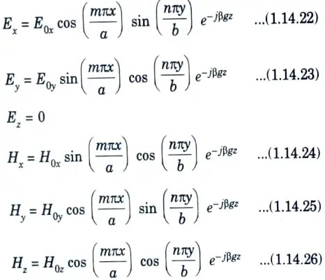
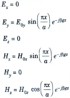
12. The field component of dominant mode (TE10) can be found by putting m = 1,n = 0 in eq. (1.14.22), eq. (1.14.23), eq. (1.14.24), eq. (1.14.25) and eq. (1.14.26).
Thus,
B. To show :
1. The TMmn mode field equation in rectangular waveguides are :
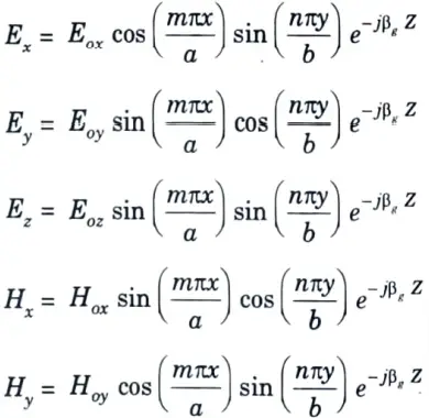
Hz = 0
i. TM01 mode: m = 0 and n = 1
If m = 0 and n = 1 are substituted in Ex, Ey, Ez, Hx and Hy, so that all of them vanishes and hence TM01 mode cannot exist.
ii. TM10 mode: Again all field components vanish and hence TM10 mode cannot exist.
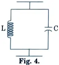
b. What is a microwave cavity resonator ? Explain it with suitable diagram and equivalent circuit. Where does it find applications ?
Ans. A. Microwave cavity resonator :
1. When one end of the waveguide is terminated in a shorting plate there will be reflections and hence standing waves as shown in Fig. 1.
2. When another shorting plate is kept at a distance of a “multiple of λg/2” then the hollow space so formed can support a signal which bounces back and forth between the two shorting plates.
3. This results in resonance and hence the hollow space is called cavity and the resonator as the cavity resonator.
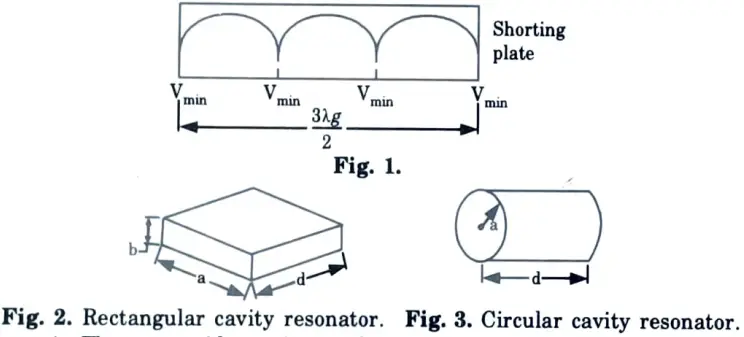
4. The waveguide section can be rectangular or circular as shown in Fig. 2 and Fig. 3.
5. The microwave cavity resonator is akin to a tuned circuit at low frequencies having a resonant frequency
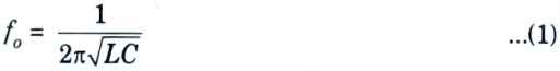
6. The cavity resonator can resonate at only one particular frequency just as a parallel resonant circuit shown in Fig. 4.
7. From Fig. 1, d = 3λg/2.
8. For a given resonator and mode a, b, m and n are constants.
9. Therefore λc is also fixed and λo will also have a fixed value.
10. But λo =f/f, and f will also have a constant value, equal to fo which is the resonant frequency of the cavity resonator.
B. Application :
1. A cavity resonator can be used as a frequency sensor.
2. Microwave cavity resonators are used in transmitters, oscillators and filters.
Section 4: Repeated Questions in Microwave and Radar Engineering
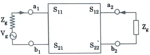
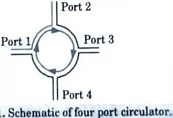
a. Why S-parameters are used at microwave frequencies to describe multiport network ? Draw the schematic diagram of four port microwave circulator and derive its S-matrix.
Ans. A. Importance of S-parameters :
1. Equipment is not readily available to measure total voltage and current at the ports of the network.
2. Short and open circuits are difficult to achieve over broadband frequencies.
3. Active devices, such as power transistors and tunnel diodes, frequently will not have stability for a short or open circuit.
4. Above difficulties can be resolved with the help of S-parameter. S-parameters can be expressed as
b1 = S11a1 S12a2
b2 = S21a1 S22a2
5. Fig. shows two port network for S-parameters.
B. Circular :
1. A microwave circulator is a multiport junction in which the wave can flow only from the nth port to the (n + 1)th port in one direction only.
2. There is no restriction on number of ports. It is a non-reciprocal device. Wave incident in port 1 is coupled into port 2 only, a wave incident in port 2 is coupled into port 3 only and so on.
3. Generally circulator is a four port device. The schematic of four ports circulator is as shown in Fig.
4. In such cases each port is connected to the next port in a clockwise direction i.e., port l is connected only to the port 2 and not to the port 3 and port 4.
5. Circulators are generally used to provide the isolation between input and output terminals in case of two terminal amplifier devices.
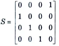
Scattering matrix of circulator :
1. A circulator shown in Fig. is made up of using two magic tees and phase shifter. The phase shifter produces a phase shift of 180°.
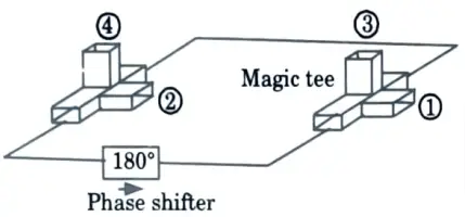
2. A perfectly matched, lossless, and non-reciprocal four port circulator has an S-matrix as
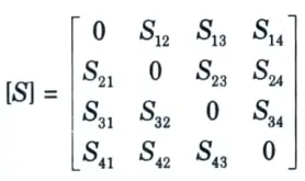
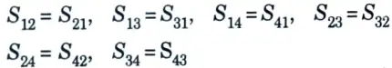
3. From the symmetry property of S-matrix
4. From the zero property of S-matrix
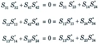
5. From the unitary property of S-matrix
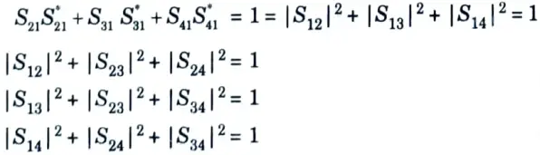
6. Now S-matrix is given as
b. Explain the operation of a Faraday rotation isolator with the help of neat sketch. List the applications of ferrite isolator.
Ans. A. Faraday rotation in ferrites :
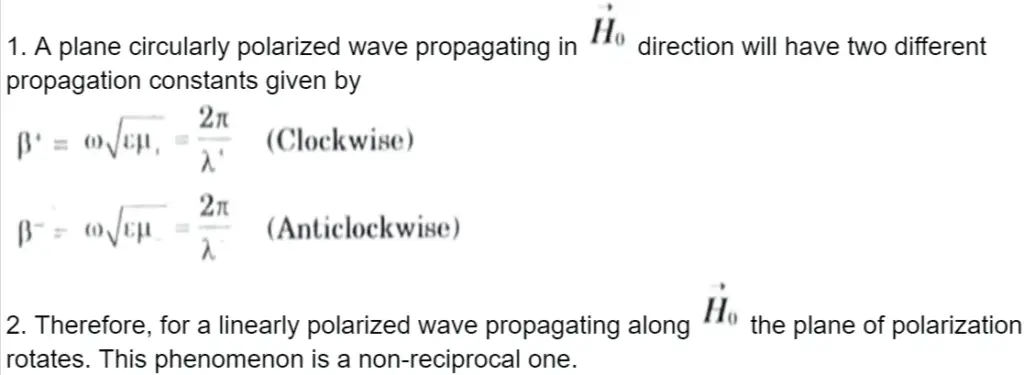
3. The rotation of the electric field of a linearly polarised wave passing through a magnetised forrite is known as Faraday rotation as shown in Fig. 2.19.1.
4. Let a linearly polarised TEM wave propagate in ferrite along the z-axis with E = xEx at z = 0. The linearly polarised wave may be decomposed into sum of clock and anti-clockwise circularly polarised waves.
5. The component waves propagate with different phase constants β+ and β– respectively, and the two corresponding electric field vectors rotate at different rates.
6. Over a distance 𝛌 the resultant linearly polarised wave will undergo a phase delay of
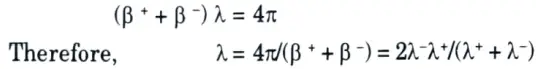
and corresponding rotation angle
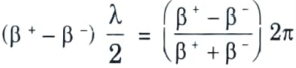
7. The rotation per unit distance is θ = (β+ – β–)/2. This property is utilised in designing ferrite isolator and circulators.
B. Faraday rotation in designing :
i. Isolator :
- 1. An isolator is a non-reciprocal transmission device used to isolate one component in a transmission line from reflections of other components.
- 2. An ideal isolator absorbs all of the power required for propagation in one direction while providing lossless transmission in the opposite direction. As a result, the isolator is commonly referred to as uniline.
ii. Operating principle and working :
- 1. The y-z plane contains the input resistive card. The output resistive card is 45° offset from the input card.
- 2. When a direct current magnetic field is applied longitudinally to a ferrite rod, it rotates the polarisation wave plane by 45°.
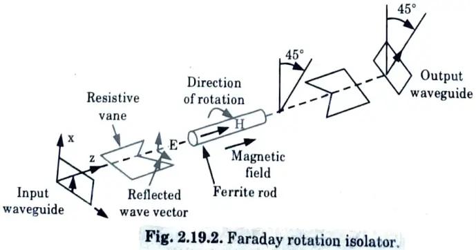
- 3. The degrees of rotation depend on the length and diameter of the rod and on the applied DC magnetic field.
- 4. An input TE10 dominant mode is incident to the left end of the isolator. As the TE10 mode wave is perpendicular to the input resistive card, so the wave passes through the ferrite rod without attenuation.
- 5. The ferrite rod section’s wave is rotated 45° clockwise and is normal to the output resistive card.
- 6. The wave arrives at the output end with no attenuation as a result of rotation.
- 7. On the other hand, the ferrite rod rotates a reflected wave from the output end clockwise 45°.
- 8. The reflected wave, on the other hand, is parallel to the input resistive card. As a result, the wave is absorbed by the input card.
- 9. The isolators typical performance is about 1 dB insertion loss in forward transmission and 20 to 30 dB isolation in reverse attenuation.
iii. Applications :
- 1. Used to improve the frequency stability of wave generator such as klystrons and magnetrons.
- 2. Used to isolate one component from reflections of other components in the transmission line.
Section 5: Notes, Questions in Microwave and Radar Engineering
a. With support of figures, explain the working of TWT. Also write its limitations.
Ans. i. Working of TWT :
- 1. Fig. depicts the physical construction of a typical TWT as well as the schematic electrode arrangement.
- 2. It has an electron gun, similar to those used in klystrons, that produces a narrow constant velocity electron beam.
- 3. A long axial helix is passed through the centre of the electron beam.
- 4. A magnetic focusing field is used to keep the beam from spreading and to guide it through the helix’s centre.
- 5. A helix is a thin conducting helical wire that is loosely wound and acts as a slow wave structure.
- 6. The signal to be amplified is applied to the helix end opposite the electron gun.
- 7. Under normal operating conditions, the amplified signal appears at the output or other end of the helix.
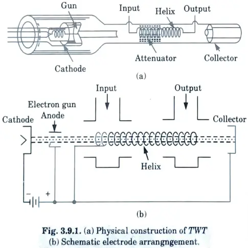
ii. Limitations :
- 1. It operates at lower efficiencies.
- 2. In coupled cavity TWT, coupling effect takes place between the cavities.
- 3. Helix TWT has limitation on high peak power due to helix wire thickness.
b. Explain the working principle of two cavity Klystron amplifier. Calculate optimum length of drift space.
Ans. i. Two cavity Klystron amplifier :
- 1. All electrons injected from the cathode travel at the same velocity to the first cavity.
- 2. Electrons passing through the first cavity gap at zero gap voltage (or signal voltage) have the same velocity as those passing through the positive half cycle of the gap voltage, while those passing through the negative half cycle of the gap voltage have a lower velocity.
- 3. As a result of these actions, electrons gradually cluster together as they travel down the drift space, as illustrated in Fig.
- 4. Velocity modulation is the variation in electron velocity in drift space. The electron density in the second cavity gap varies cyclically with time.
- 5. During the retarding phase, the maximum bunching occurs approximately halfway between the second cavity grids. Thus, the electrons’ kinetic energy is transferred to the field of the second cavity.
- 6. The electrons then exit the second cavity at a lower velocity and arrive at the collector.
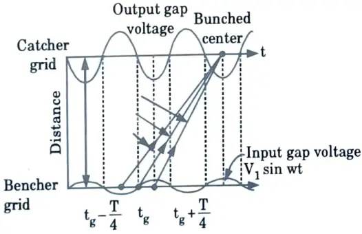
ii. Optimum length of drift space :
1. From the basic principles, we can say that the klystron is generally tuned to fundamental AC component of current given by,

where, t3 = Time when the bunched electrons are at the catheter grid after travelling through the field free drift space L.
𝛉g = Transit angle = ωtg = ω(t2 – t1)
t1 = Time when electron beam enters the buncher.
t2 = Time when electron beam out.
I0 = DC beam current in the buncher.
2. Here J1(X) is a function of V0 because
where,
β1 = Beam coupling coefficient of buncher cavity.
V1 = Input RF signal amplitude.
V0 = Anode potential with respect to cathode potential.
N = Number of RF cycles elapsed during transit time of reference electron with velocity (u,).
For maximum optimum drift space length,
X= 1.841
Section 6: Featured Questions in Microwave and Radar Engineering
a. Discuss the salient features of microwave measurements. Describe a voltage standing wave ratio (VSWR) meter.
Ans. i. Salient features of microwave measurements :
- 1. It is easier to measure voltage and current at low frequencies and use them to calculate power.
- 2. However, at microwave frequencies, they are difficult to measure and, because they vary with transmission line position, are of little use in determining power. As a result, at microwave frequencies, measuring power directly is more desirable and simpler.
- 3. Circuits at low frequencies use lumped elements that can be identified and measured. Because circuit elements are distributed at microwave frequencies, it is usually not necessary to know which element makes up a line.
- 4. Measuring the impedance of a circuit without regard to the individual distributed elements that comprise that circuit is both possible and satisfactory.
- 5. Unlike low frequency measurements, many quantities measured at microwave frequencies are relative, and their absolute values are not required.
- 6. Furthermore, for power measurement, knowing the ratio of two powers (or their difference in dBs) rather than exact input or output powers is usually sufficient.
ii. Voltage standing wave ratio (VSWR) meter :
- 1. It is sensitive, high gain, high Q, low noise voltage amplifier tuned normally at a fixed frequency of 1 kHz at which the microwave signal is modulated.
- 2. The input of the VSWR meter is the detected signal output of the microwave detector and the output of the amplifier is measured with a square law wave calibrated voltmeter.
- 3. This voltmeter directly gives the VSWR reading Vmax/Vmin for an input of Vmin after the meter is adjusted to unity VSWR for an input corresponding to Vmax. A gain control can be used to adjust the reading to desired value.
- 4. There are mainly three scales on VSWR meter
- i. The normal SWR scale can be used when VSWR is between 1 and 4.
- ii. The bottom of normal SWR scale can be used when the VSWR is between 3 and 10.
- iii. The expanded SWR scale can be used when the VSWR is less than 1.3.
b. What are various methods for measuring frequency ? Discuss in detail.
Ans. A. Measuring frequency using frequency counter :
- 1. The schematic for this method is shown in Fig. A directional coupler is placed between the frequency generator and the adjustable attenuator.
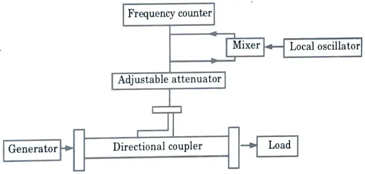
- 2. A portion of the input microwave signal is sampled by this directional coupler and passed to the adjustable attenuator.
- 3. The adjustable attenuator is used to reduce power passing to the frequency counter by attenuating some of the microwave signal.
- 4. The frequency counter then measures the frequency of the incoming signal directly.
- 5. The mixer and local oscillator are used to extend the frequency counter’s range.
B. Beat Frequency Measurement Method :
- 1. The arrangement for measuring beat frequency is shown in Fig., and the sweep generator is used to sweep the oscilloscope’s horizontal input.
- 2. After attenuating the signal, the adjustable attenuator sends it to the wavemeter.
- 3. The wavemeter and harmonic generator send the signal to the mixer via the directional coupler, and the mixer outputs the difference frequency, one of which is eliminated by the low pass filter.
- 4. This signal through detector used to control the horizontal input of oscillator.
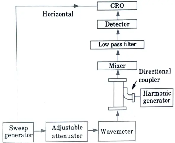
- 5. The amplitude level corresponding to the difference in sweep generator and harmonic frequency is now obtained on the oscilloscope.
- 6. The amplitude change as frequency changes and becomes zero at zero beat.
Section 7: Mechanical Engineering Question in Microwave and Radar Engineering
a. Derive expression for probability of false alarm in radar.
Ans. 1. The noise at the input to the IF filter can be described by the Gaussian probability function which is given as
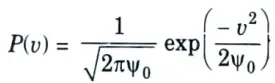
where, P(v) du is the probability of finding the Loise voltage between v and v + dv and ψ0 is the mean square value of the noise voltage.
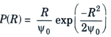
2. When the Gaussian noise is passed through the IF filter, the probability density function (PDF) is given in a form of Rayleigh PDF:
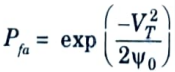
3. When the noise voltage will exceed the threshold voltage VT, then the probability is evaluated from VT to ∞ or
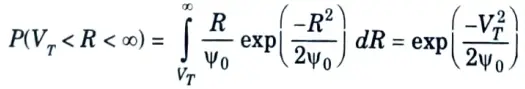
4. This is the probability of false-alarm since it represents the probability that noise will cross the threshold and be called a target when only noise is present. Thus,
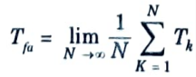
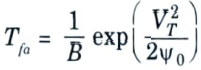
5. The false-alarm time Tfa is defined as the average time between crossings of the decision threshold when noise alone is present, and is given by
6. The false alarm probability is the ratio of the time the envelope is above the threshold to the total time.
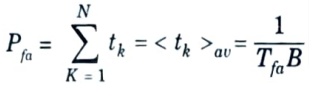
7. The average of Tk is the false-alarm time, Tfa
8. When the number of cognitive radios increases, the miss probability becomes smaller for any given false-alarm probability.
9. This implies that the false-alarm probability cannot be sufficiently small due to the bound. The false-alarm wall results from the reporting error probability (Pe), which characterizes the error probability when the sensing result is transmitted from one cognitive radio to the common receiver over an imperfect result.
b. Draw block diagram and explain the operation of MTI radar.
Ans. A. MTI radar :
- 1. The block diagram of MTI radar is shown in Fig. Here the MTI radar is employing a power amplifier as the transmitter.
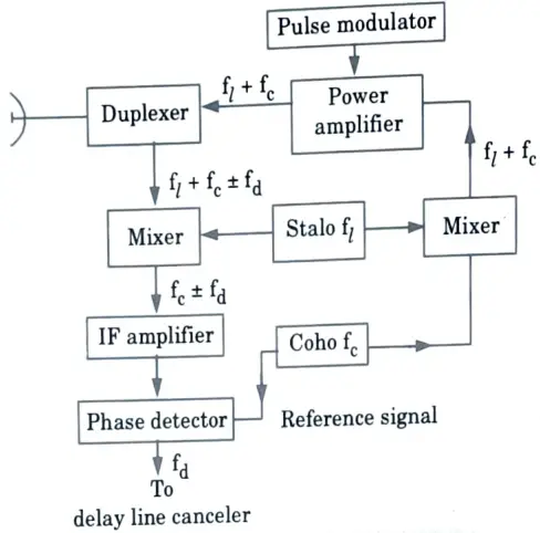
- 2. The local oscillator of the MTI radar’s superheterodyne receiver is more stable than the local oscillator in this case.
- 3. To recognise the need for high stability, an MTI receiver’s local oscillator is referred to as the stalo, which stands for stable local oscillator. The IF amplifier is intended to function as a matched filter.
- 4. Instead of an amplitude detector, a phase detector is used after the IF stage. It is a mixer-like device that combines the received signal (at IF) and the reference signal from the echo to generate the difference in frequencies between the received signal and the reference signal. This is known as the Doppler frequency.
- 5. The name coho stands for coherent oscillator to signify that it is a reference signal that has the phase of the transmitter signal.
- 6. The sum of the stalo and coho signals as the input signal to the power amplifier gives the coherency.
- 7. The transmitter frequency is the sum of the stalo frequency fl and coho frequency (fc).
- 8. The combination of the stalo and coho is called the receiver exciter portion of the MTI radar.
- 9. The power amplifier is a good transmitter for MTI radar since it has high stability and is capable of high power.
- 10. The pulse modulator turns the amplifier on and off to generate radar pulse.
B. Applications of MTI Radar :
- 1. It is used for both land-based and airborne MTI applications.
- 2. It has been used to detect moving ground vehicles with a side-looking airborne radar.