
Use our AKTU question paper and solution for a journey into the world of Optical Communication. Explore fascinating ideas and learn insightful lessons with these thorough and educational notes.
Dudes 🤔.. You want more useful details regarding this subject. Please keep in mind this as well.

Important Questions For Optical Communication:
*Quantum          *B.tech-Syllabus
*Circulars           *B.tech AKTU RESULT
* Btech 3rd Year
Section A: Optical Communication Short Notes
a. Define acceptance angle and numerical aperture.
Ans.
- A. Acceptance angle: The acceptance angle is the maximum angle to the axis at which light may enter the fiber in order to propagate.
- B. Numerical aperture: The numerical aperture (NA) of a fiber is defined as the sine of the maximum angle an incident ray can have for total internal reflection in the core.
b. Explain normalized frequency (V) value in a multimode and single mode optical fiber.
Ans. 1. Normalized frequency is a dimensionless quantity, denoted by V, given by:
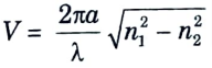
2. For a single mode fiber, it is required that normalized frequency, satisfy the condition V < 2.4048.
3. The mode volume of a multimode fiber, which is the approximate number of bound modes within the fiber, is directionally proportional to the normalized frequency.
c. Classify different types of nonlinear scattering in an optical fiber.
Ans. This type of scattering are of two types:
- i. Stimulated Brillouin Scattering (SBS):
- 1. SBS can be defined as light modulation via thermal molecular vibrations within the fiber.
- 2. The dispersed light appears as upper and lower side bands separated by the modulation frequency from the incident light.
- ii. Stimulated Raman Scattering (SRS):
- 1. This type of scattering is comparable to Stimulated Brillouin Scattering (SBS), except that the scattering process generates a high frequency optical phonon rather than an acoustic phonon.
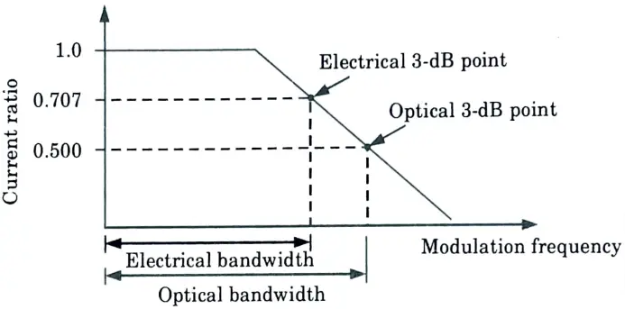
d. Differentiate between electrical and optical bandwidth using frequency response curve.
Ans.
| S. No. | Electrical bandwidth | Optical bandwidth |
| 1. | It is defined as the frequency at which the ratio of current output to current input falls to 0.707. | It is the frequency at which the power output to power input ratio falls to 0.5. |
The frequency response of optical source is shown in Fig.
e. Explain the importance of double hetereo-junction structures in an optical souree.
Ans. Importance of double hetereo-junction structure are:
- 1. It offers higher efficiency with low to high radiance compare to single homojunction (p-n+) LED type.
- 2. Emitting wave length of GaAs / Al GaAs based DH LEDs range approximately between 0.8 to 0.9 um.
- 3. n-region and p-region can be highly doped.
f. Plot the effect of temperature on the avalanche gain of a photodiode.
Ans.
- 1. Due to the temperature dependency of the electron and hole ionization rates, the gain mechanism of an avalanche photodiode is extremely temperature sensitive.
- 2. This temperature dependence is especially important at high bias voltages, when tiny temperature changes can produce huge fluctuations in gain.
- 3. Consider a silicon avalanche photodiode as an example. If the operating temperature is reduced while the applied bias voltage remains constant, the ionization rates for electrons and holes rise, as does the avalanche gain.
- 4. The electric field in the multiplication area of the p-n junction must be modified to maintain a consistent gain when the temperature changes.
- 5. To do this, the receiver must have a compensation circuit that adjusts the applied bias voltage on the photodetector as the temperature varies.
g. Define receiver sensitivity and quantum limit.
Ans. Receiver sensitivity: A particular minimum average optical power level must arrive at the photodetector to achieve the appropriate BER for a given data rate. The receiver sensitivity is the value of this minimum power level.
Quantum limit: For an ideal photo detector quantum efficiency 𝜂 = l and has zero dark current then the minimum received. Power for a specific bit-error rate is known as quantum limit.
h. Define intrinsic and extrinsic absorption in an optical fiber.
Ans. A. Intrinsic absorption: It is created by the interaction of the propagating light wave with one or more of the primary components of glass that make up the material composition of the fiber.
Extrinsic absorption:
- 1. Impurities in the fiber substance produce it.
- 2. Extrinsic absorption is generated by the metal ions’ electronic shift from one energy level to another.
i. Formulate the condition of minimum gain in Fabry-Perot cavity to sustain oscillation.
Ans.
- 1. A gain medium would be put between the two high-reflectivity (≈ 100 %) mirrors of a Fabry-Perot interferometer so that a coherent wave could be constructed after several round trips of the light through the amplifier.
- 2. After the inverted population was created in the gain medium at the start of the device, a unique spontaneously emitted photon moving along the cavity axis would begin stimulated emission, increasing the number of coherent photons.
- 3. If the gain was more than the losses after a round trip between the mirrors, the intensity of the visible electromagnetic wave would increase as an exponential function after each round trip, and a self-sustaining oscillation would begin.
j. Define stimulated emission.
Ans. A photon with an energy equal to (E2 – E1) interacts with the atom in the higher energy state, forcing it to revert to the lower energy state and generate a second photon.
Section B: Optical Communication Important Notes
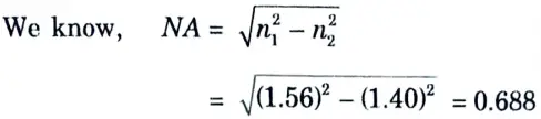
a. Find out the relationship between acceptance angle and refractive indices of core, cladding and medium for a light ray incident on the fiber core. Calculate the numerical aperture of step index fiber having core refractive index of 1.56 and cladding refractive index as 1.40.
Ans. Acceptance angle :
- 1. The geometry concerned with launching a light ray into an optical fiber is shown in Fig.
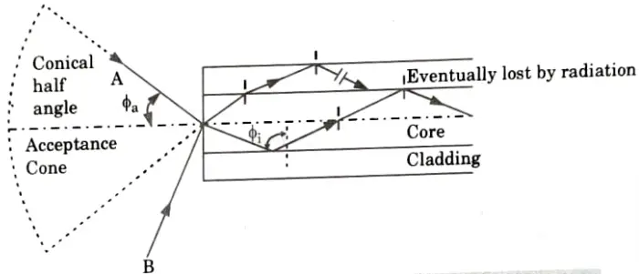
- 2. In this, it is observed that the meridional ray ‘A’ enters the fiber core at refracted at the air core interface an angle 𝜃a to the fiber axis and before transmission to the core-cladding interface at the critical angle.
- 3. Thus, any ray which is incident into the fiber core at an angle greater than 𝜃a will be transmitted to the core-cladding interface at an angle less than 𝜃c, and will not be totally internally reflected.
- 4. In the Fig. it is observed that incident ray B at an angle greater than 𝜃a is refracted into the cladding and eventually lost by radiation.
- 5. Thus 𝜃a is the maximum angle to the axis at which light may enter the fiber in the order to be propagated, and is referred as acceptance angle.
B. Numerical:
Given: n1 = 1.56, n2 = 140
To Find: Numerical aperture
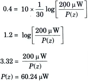
b. Define attenuation. Consider a 30 km long optical fiber working at wavelength (𝛌) of 130 nm and has an attenuation of 0.4 dB/km, find out the output optical power if 200 𝛍W of optical power is launched into the fiber.
Ans. A. Attenuation:
- 1. Attenuation is a measure of decay of signal strength or loss of light power that occurs as light pulses propagate through the length of the fiber.
- 2. Signal attenuation within optical fibers is usually expressed in the logarithmic unit of decibel (dB).
- 3. dB is used to compare two power levels, may be defined for a particular optical wavelength in the ratio of the input power pi into a fiber to the output optical power po from the fiber as
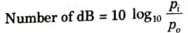
- 4. In optical fiber communication the attenuation usually expressed in dB per km.
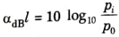
where 𝛼dB is signal attenuation per unit length in dB and l is the length of the fiber.
B. Numerical:
Given: Z = 30 m, 𝛼 = 0.4 dB/km, Optical power = 200 𝛍W
To Find: Output optical power.
Attenuation in optical fiber is given by,
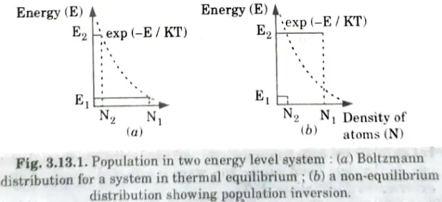
c. Define population inversion. Also derive the threshold condition for laser oscillations to sustain.
Ans. A. Population inversion:
- 1. Under thermal equilibrium condition by Boltzmann’s law, the lower energy level E1 contains more atoms than upper energy level E2.
- 2. Thus, to achieve optical amplification it is necessary to create a non-equilibrium distributions of atoms such that population of the upper energy level is greater than that of lower energy level (N2 > N1). This is known as population inversion.
- 3. Thus in order to achieve population inversion, it is necessary to excite atoms into upper energy level E2 and hence obtain a non-equilibrium distribution. This process is achieved by using an external energy source referred as ‘pumping’.
B. Derivation the threshold condition for laser oscillations:
- 1. The steady state condition is achieved when the gain in the amplifying medium precisely balances the losses.
- 2. Although population inversion is required for oscillation to occur, a minimum or threshold gain is also required.
- 3. All losses due to transmission through the mirror may be included in a single loss coefficient 𝛼 per cm.
- 4. Let assume the amplifying medium occupies a length L completely filling the region between the two mirrors which have reflectivities r1 and r2.
- 5. On each round trip beam passes through the medium twice. Hence the fractional loss experienced by the light beam is

- 6. If the gain coefficient per cm is g, the fractional gain in the round trip is
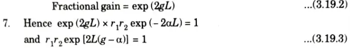
8. Threshold gain gth per cm may be obtained by rearranging the expression
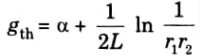
9. The second term on RHS represents transmission loss through mirrors.
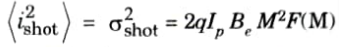
d. Explain the possible noise sources in a photodiode. Also explain quantum noise in detail.
Ans. Noise sources in optical fiber communication are:
1. Quantum or shot noise: It results from the stochastic character of the generation or collection of photoelectrons when an optical signal strikes a photodetector. The shot noise current has a mean square value in a receiver bandwidth BC which is proportional to average value of photocurrent Ip.
2. Dark current noise generated in bulk material of a photo diode: The bulk dark current iDB arises from electrons or holes which are thermally generated in the p-n junction photodiode. The mean square value of this current is given by
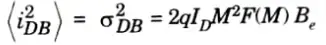
3. Surface dark current/surface leakage current: Surface flaws, cleanliness, bias voltage, and surface area all have a role. A guard ring arrangement that shunts surface leakage current away from the load resistor is an effective approach to reduce dark current.
The mean square value of dark current is
e. Discuss free space optics (FSO) based communication systems.
Ans.
- 1. FSO communication systems use free space as a communication route between transceivers that are in line-of-sight (LOS) for successful optical signal transmission.
- 2. The channel, which might be atmosphere, space, or vacuum, determines the transmission and reception of optical signals in order to construct dependable and efficient communication systems.
- 3. Data is exchanged using FSO technology via light propagation over atmospheric or space communication channels, allowing optical connectivity.
- 4. FSO communication provides a high data rate to fulfill the rapidly growing need for broadband traffic, which is primarily driven by Internet access and HDTV broadcasting services.
- 5. When compared to fiber optics technology, FSO provides significantly more freedom in creating optical network designs at very high speeds, ranging from tens to hundreds of Gbit/s.
- 6. Nevertheless, atmospheric influences limit sensitivity and attainable data rates with tolerable BER in FSO transmission.
- 7. FSO communication is the most realistic solution to the bottleneck problem in broadband connectivity. FSO lines’ data rates continue to rise in both long- and short-range applications.
- 8. FSO will be one of the most distinctive and powerful methods for addressing connectivity bottlenecks that have developed in high-speed networks over the last decade as a result of the Internet’s remarkable success and sustained popularity.
Section 3: Core Refractive Index Profile
a. Classify optical fibers on the basis of number of modes and core refractive index profile.
Ans. A. Mode Coupling:
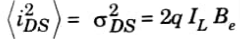
- 1. Waveguide perturbations such as fibre axis deviations from straightness, core diameter variations, abnormalities at the core cladding interface, and refractive index fluctuations can all modify the propagation characteristics of the fibre.
- 2. Depending on the specific perturbation, these will have the effect of coupling energy going in one mode to another.
- 3. Ray theory assists understanding of this event, as illustrated in Fig., which depicts two types of disturbance. It can be seen that the beam no longer maintains the same angle with the axis in both circumstances.
- 4. In electromagnetic wave theory, this refers to a change in the light’s propagation mode.
- 5. As a result, even when the fibre is of great quality and is neither stretched or bent by its surroundings, individual modes do not generally propagate along the length of the fibre without substantial energy transfers to adjacent modes. Mode coupling or mixing refers to this mode conversion.
- 6. Mode coupling influences fibre transmission qualities in a variety of ways, the most significant of which being the dispersive properties of fibres over long distances.
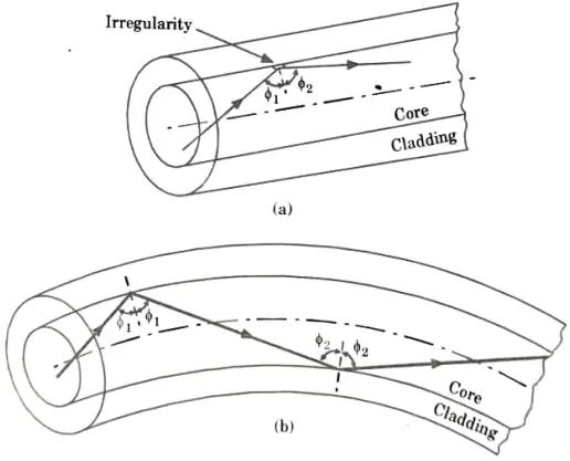
B. Step Index Fiber:
- 1. A step index fiber is one for which the refractive index of core n1 is constant and is larger than the refractive index of the cladding n2.
- 2. The refractive index profile for this type of fiber makes a step change at the core-cladding interface that’s why it is named as step index fiber.
- 3. The refractive index profile may be defined as :
- 4. There are two major types of step index fiber
- a. Multimode step index fiber
- b. Single mode step index fiber.
- 5. The Fig. shows a multimode step index fiber and single mode step fiber. In multimode step index fiber core diameter is around 50 𝛍m or greater, which is large enough to allow the propagation of many modes within the fiber whereas single mode step index fiber has a very fine thin core, so that only one mode can be propagated.
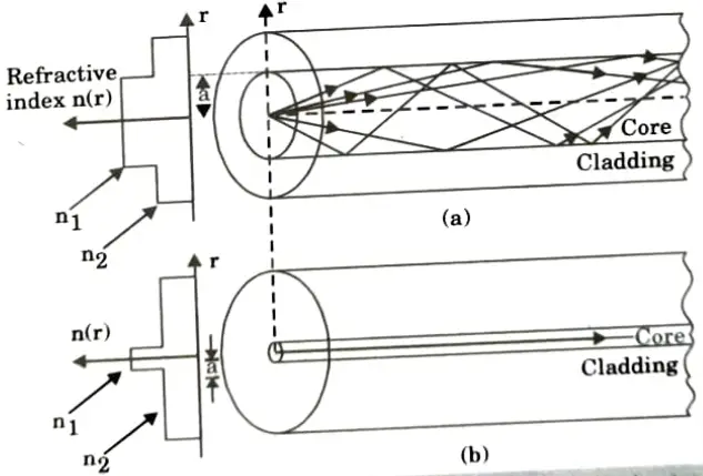
- 6. Multimode step index fiber allows the propagation of finite number of guided modes along the channel.
- 7. The number of guided modes is dependent upon the physical parameters of the fiber and the wavelengths of the transmitted light which are included in the normalized frequency V of fiber.
- 8. The eq. (1.20.1) can also be written in form
- 9. Guided modes are important in optical fiber communications as these are confined to fiber over its full length.
- 10. The total number of guided modes is also known as mode volume (MS).
- 11. For step index fiber,

- 12. For single mode fiber V < 2.405 and for multimode fiber V > 2.405.
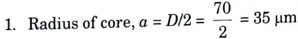
b. A multimode step index fiber with core diameter of 70 𝛍m, relative refractive index difference of 1.7% is operating at a wavelength of 0.85 𝛍m. If the core refractive index is 1.48, estimate
i. Normalized frequency
ii. Number of guided modes.
Ans. Given: D = 70 𝛍m, 𝚫 = 1.7% = 0.017, 𝛌 = 0.85 𝛍m, n1 = 1.48
To Find: Normalized frequency V, Number of guided modes.
2. Normalized frequency of fiber is,
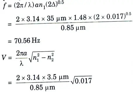
= 33.715
3. The number of guided modes,
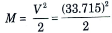
M = 568
Section 4: Optical Communication Important Numerical
a. Determine the rms pulse broadening (𝛔s) due to intermodal dispersion in terms of core refractive index (n1), cladding refractive index (n2) and the length of fiber for a multimode step index fiber. A 6 km optical link consists of multimode step index fiber with a core refractive index of 1.5 and a relative refractive index difference of 1%. Estimate the delay difference between the slowest and fastest modes.
Ans. Given: L = 6 km, n1 = 1.5, 𝚫 = 0.01
To Find: RMS pulse broadening (𝛔s), delay difference between the slowest and fastest modes.
1. RMS pulse broadening is given by,
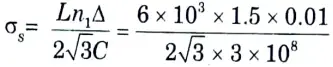
= 8.66 x 10⁻⁸m = 86.6 nm
2. Delay difference between the slowest and fastest modes is,
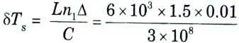
= 30 x 10-8 = 0.30 𝛍s
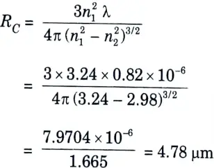
b. Explain the bending losses in an optical fiber, also calculate the critical radius of curvature for a multimode fiber with a core refractive index of 1.8, a relative refractive index difference of 4 % and an operating wavelength of 0.82 𝛍m.
Ans. A. Bending loss:
- 1. Radiation losses occur in optical fibers at bends or curves in their courses. The energy in the evanescent field at the bend exceeds the velocity of light in the cladding, causing the guidance mechanism to be stopped and light energy to be radiated from the fiber.
- 2. The section of the mode on the outside of the bend must travel faster than the part on the inside in order to maintain a wavefront perpendicular to the direction of propagation.
- 3. As a result, a portion of the mode in the cladding must travel faster than the speed of light in that medium.
- 4. The loss can generally be represented by the radiation attenuation coefficient which is given as:

where R is the radius of curvature of the fiber bend,
C1 C2 are constants and are independent of R.
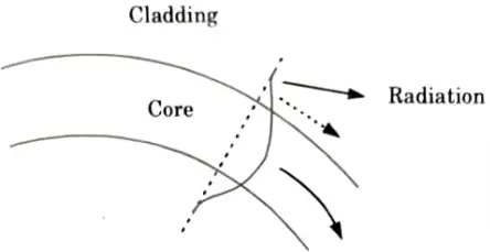
5. Large bending losses tend to occur in multimode fibers at a critical radius of curvature RC, which is given by
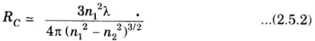
6. From eq. (2.5.2), it is observed that potential macro bending losses may be reduced by:
a. Designing fibers with large relative refractive index difference.
b. Operating at the shortest wavelength possible.
7. The critical radius of curvature fora single mode fiber RCS is given by:
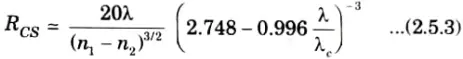
where 𝛌C is the cut-off wavelength for the single mode fiber.
8. Thus, for single mode fiber, the critical wavelength of the radiated light becomes progressively shorter as the bend radius is decreased. The critical radius is called critical bending radius.
B. Numerical:
Given: n1 = 1.8, 𝚫 = 0.04, 𝛌 = 0.82 𝛍m
To Find: Critical radius of curvature RC
= 2.98
2. Critical radius of curvature for a multimode fiber is,
Section 5: S-LED and E-LED Structures
a. Explain Fabry Perot resonating cavity. A ruby laser contains a crystal of length 5 cm with a refractive index of 1.67. The peak emission wavelength from the device is 0.65 𝛍m. Determine the no of longitudinal modes and their frequency separation.
Ans. A. Fabry Perot resonating cavity:
- 1. Figure displays a laser diode made up of two mirrors and an active medium between them. A resonator of length L is formed by two mirrors.
- 2. Let an arbitrary wave to travel from the left mirror to the right mirror. This wave is reflected at the right hand mirror, resulting in a 180° phase shift.
- 3. As seen in Fig.(b), the wave should have a break in its phase, which is impossible in this case. In other words, this resonator is incapable of supporting this wave.
- 4. Consider another wave travelling inside a resonator, as illustrated in Fig (c).
- 5. The wave undergoes a 180° phase change at the right mirror and continues to propagate. This wave has the same phase shift and continues to move in the left mirror. As a result, this wave produces a steady pattern known as a standing wave.
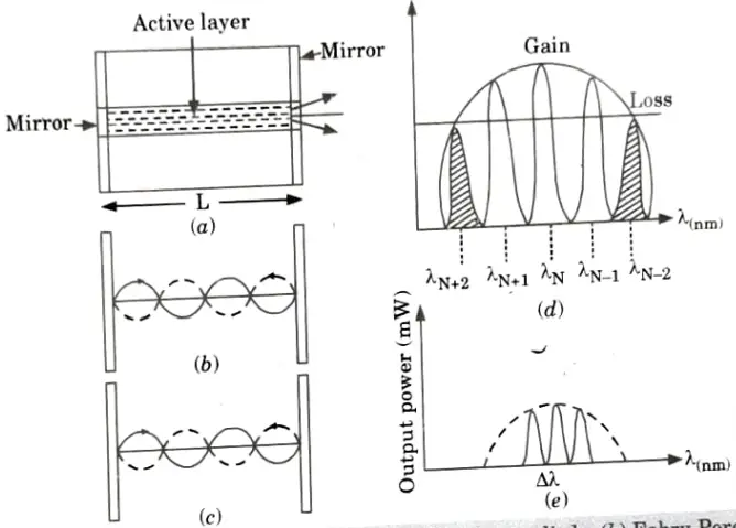
- 6. Two waves shown in Fig.(b) and (c) differs in their wavelength. Thus, a resonator can support only a wave with a certain wavelength, the wave that forms a standing wave pattern.
- 7. This physical requirement can be written as:
- 8. This resonator supports a wavelength equal to

and so forth. Wavelengths selected by a resonator are called longitudinal modes.
- 9. The laser shifts from one longitudinal mode to another when the length of a resonator increases or decreases. This is known as mode hop.
- 10. A resonator can support an infinite number of waves whose wavelengths satisfy eq. (3.14.1.). However, the active medium provides gain within only a sm¡ll range of wavelengths.
- 11. Because a laser is made up of a resonator and an active medium, and radiation is the result of their interaction, only a few resonant wavelengths within the gain curve may be radiated. This is depicted in Fig (d).
- 12. Only when gain outweighs loss does light appear. As a result, only resonant wavelengths inside the gain over loss curve will eventually be emitted.
13. Waves with 𝛌N, 𝛌N ±1 and 𝛌N ±2 might be radiated, but only waves with 𝛌N and 𝛌N ±1 will be the actual laser output. Modes 𝛌N ±2 Shown black, are not generated. - 14. More specifically, we can explain this by introducing the spacing between two adjacent longitudinal modes, 𝛌N – 𝛌N ±1.
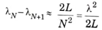
B. Numerical:
Given: L = 0.05 m, n = 1.67, 𝛌 = 0.65 𝛍m
To Find: Number of longitudinal modes, frequency separation
1. The number of longitudinal modes is given by,
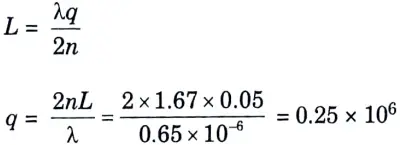
2. The frequency separation of modes is,
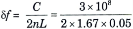
= 1.79 GHz
b. Explain S-LED and E-LED structures with the help of proper diagram.
Ans. Types of LED structure:
a. Planar LED:
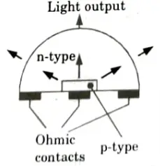
- 1. The planar LED is the most basic structure accessible, and it is manufactured using either liquid or vapour phase epitaxial techniques across the entire surface of a GaAs substrate.
- 2. To generate the junction seen in Fig. 2, p-type diffusion into the n-type substrate is used. Lambertian spontaneous emission results from forward current flow through the junction, and the gadget emits light from all surfaces.
b. Dome LED:
- 1. An n-type GaAs hemisphere is generated surrounding a diffused p-type area.
- 2. The dome’s diameter is selected to maximize the quantity of internal emission reaching the surface within the critical angle of the GaAs-air interface.
- 3. As a result, this gadget uses less external power than a planar LED.
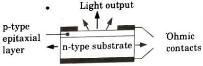
c. Surface emitter LEDs:
- 1. The structure of a high radiance etched well DH surface emitter for the 0.8 to 0.9 mm wavelength band is shown in Fig.
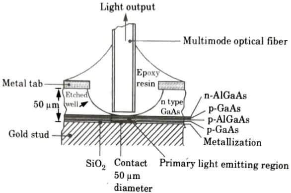
- 2. The internal absorption of this device is very low due to large bandgap confining layers, and the reflection coefficient at the back crystal face is high giving good forward radiance. The power coupled PC into a multimode step index fiber may be estimated as:
- 3. The addition of epoxy resin to the etched well reduces the refractive index mismatch and increases the device’s external power efficiency.
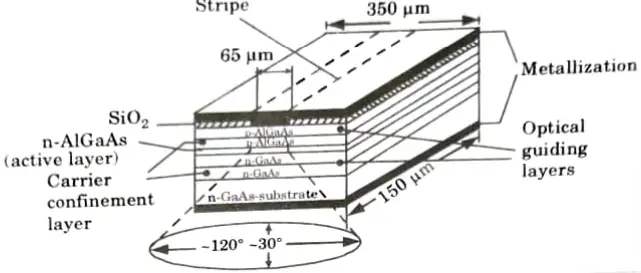
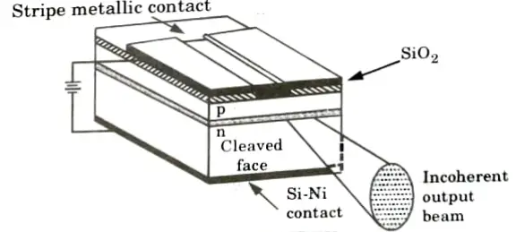
d. Edge emitter LEDs:
- 1. Stripe geometry DH edge emitter LED is the basic high radiance configuration now employed in fiber transmission (ELED).
- 2. The edge emitter shown in Fig. is made up of an active junction region, which is the source of incoherent light, and two guiding layers.
- 3. The refractive index of the guiding layers is lower than that of the active region but greater than that of the surrounding material.
- 4. This construction creates a waveguide channel, which directs optical radiation to the fiber core.
- 5. To match the typical fiber core diameter (50 – 100 mm), the contact stripes for the edge emitter are 50 -70 mm wide.
- 6. The emission pattern of the edge emitter is more directional than that of the surface emitter.
e. Superluminescent LEDs:
- 1. The third device geometry which provides significant benefits over SLED and ELED in communication applications is the superluminescent diode or SLID.
- 2. This device gives:
- i. More output power
- ii. A directional output beam
- iii. A narrow spectral bandwidth
- 3. SLD structures are long rectangular stripes, ridge waveguides, or buried heterostructures.
- 4. To prevent reflections and so suppress lasing, one end of the device is made optically lossy, with the output coming from the other end.
- 5. Fig. suppresses laser action by combining a contact stripe with an absorbing area at one end.
- 6. In pulsed mode, this device has a peak output of 60 mW and a wavelength of 0.87 mm.
- 7. To suppress lasing action, AR coating is applied to the cleaved facets of SLDs.
Section 6: Avalanche Photodiode
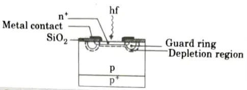
a. Explain principle, construction and working of p-i-n diode. Discuss the factors which limit the speed of response of a photodiode.
Ans. A. Working principle of photodiode (Photodetector):
- 1. A larger depletion region is required to allow operation at longer wavelengths where light penetrates deeper into the semiconductor material.
- 2. For this purpose n-type material is doped so lightly that it can be considered intrinsic and to make a low resistance contact highly doped n-type (n+) layer is added. This creates a p-i-n structure where all the absorption takes place in the depletion region.
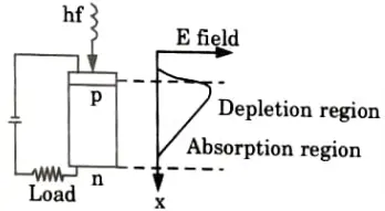
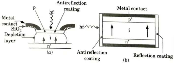
- 3. Fig. shows the structure of two types of silicon p-i-n photodiode for operation in the shorter wavelength band below 1.09 𝛍m.
- 4. When operating in the 0.8 to 0.9 𝛍m band, the front lit photodiode requires a depletion region of between 20 and 50 m to provide high quantum efficiency, fast responsiveness, and low dark current.
B. Three main factors that limit the speed of response of a photodiode are:
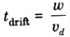
a. Drift time of carriers through the depletion region:
- 1. The speed of response of a photodiode is limited by the time it takes photogenerated carriers to drift across the depletion region. When the field in the depletion region exceeds the saturation value then the carriers may assumed to travel at constant vd.
- 2. The transit time tdrift, for carriers which must traverse the full depletion layer width w is given by
b. Diffusion time of carriers generated outside the depletion region:
Carrier diffusion is a slow process where the time taken tdiff, for carriers to diffuse a distance d may be written as
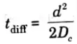
where Dc is the minority carrier diffusion coefficient
c. Time constant incurred by the capacitance of the photodiode with its load:
- 1. A reverse biased photodiode exhibits a voltage dependent capacitance caused by the variation in the stored charge at the junction. The junction capacitance Cj is given by
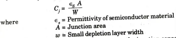
- 2. The small depletion layer width w increases the junction capacitance. The capacitance of the photodiode Cd is that of junction together with the capacitance of the leads and packaging.
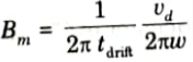
- 3. The maximum photodiode Bm is given by:
Significance:
- 1. The intrinsic layer of a PIN photodiode is important because it controls the breadth of the depletion region.
- 2. The appropriate width is selected as a compromise between sensitivity and response speed.
- 3. If the width of the depletion layer is broad, the majority of incident photons will be absorbed in the depletion zone, resulting in high sensitivity and low junction capacitance, lowering the RC time constant of the detector circuit.
b. Discuss the requirements of an ideal photo detector, also explain the construction and working of avalanche photodiode.
Ans. A. Requirements of an ideal photo detector: Photodetectors used for optical fiber communication must fulfill the following requirements for good performance:
- 1. The working wavelengths’ sensitivity should be quite high.
- 2. To accurately duplicate the received signal waveform, the photodetector response must be linear with respect to the optical signal over a wide range during analogous transmission.
- 3. The photodetector should provide the most electrical signal for a given amount of optical power, indicating a high quantum efficiency.
- 4. Response time should be as short as feasible in order to acquire an acceptable bandwidth.
- 5. Low dark currents, leakage currents, and shunt conductance. Noise in the circuits must be kept to a minimum.
- 6. The performance characteristics of an ideal detector should be independent of changes in ambient conditions.
- 7. The detector to be used must be of small size in order to have efficient coupling with fiber.
- 8. The detector should be reliable i.e., it must be capable of continuous stable operation at room temperature for many years.
- 9. It must be of low cost.
B. Avalanche photodiode:
- 1. The second major type of optical communication detector is avalanche photodiode.
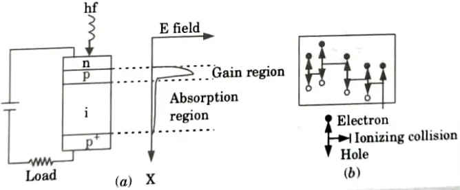
- 2. The depletion area, where most photons are absorbed and primary carrier pairs are formed, has a high field region where holes and electrons can gain enough energy to excite new electron-hole pairs.
- 3. Impact ionization is the phenomena that causes avalanche breakdown in conventional reverse biassed diodes.
- 4. To assure uniformity of carrier multiplication across the entire area, carrier multiplication factors as high as 104 can be attained utilizing defect-free materials.
- 5. High-speed operation of these devices necessitates complete depletion of the absorption zone.
- 6. When carriers are created in an undepleted medium, the diffusion process collects them slowly.
Section 7: Types of Power Penalties
a. Discuss eye pattern features in an optical communication, also comment on ISI using eye diagram.
Ans. A. Eye diagram:
1. The eye diagram is a powerful measurement tool for evaluating a digital transmission system’s data handling capability.
2. This method has been widely used to assess the performance of wire line systems and is also applicable to optical fiber data lines.
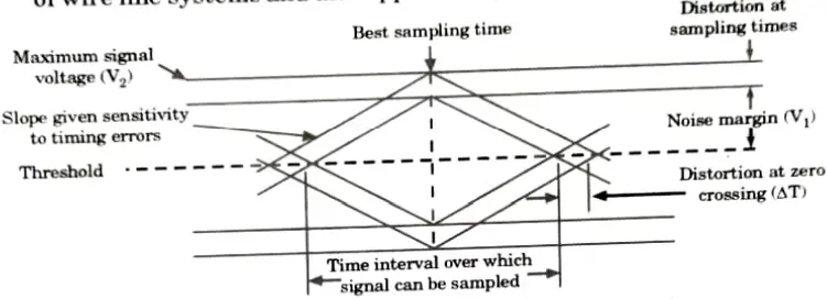
B. Eye pattern features:
- 1. The eye pattern measurements are conducted in the time domain, thus the effects of waveform distortion can be seen on the display screen of standard BER test equipment right away.
- 2. Fig. shows a typical display pattern, which is known as an eye pattern or an eye diagram. The basic upper and lower bounds are determined by the logic one and zero levels, shown by bon and boff respectively.
- 3. The following information regarding the signal amplitude distortion. timing jitter, and system rise time can be derived:
- i. The eye opening width defines the temporal interval over which the received signal can be sampled without mistake owing to interference from adjacent pulses (known as intersymbol interference).
- ii. The optimal time to sample the received waveform is when the eye opening is at its highest point. The amplitude distortion in the data transmission reduces this height. The degree of distortion is determined by the vertical distance between the top of the eye opening and the highest signal level. The harder it is to discriminate between ones and zeros in the signal as the eye closes.
- iii. The height of the eye opening at the specified sampling time shows the noise margin or immunity to noise. Noise margin is the percentage ratio of the peak signal voltage V1 for an alternating bit sequence (defined by the height of the eye opening) to the maximum signal voltage V2 as measured from the threshold level, as shown in Fig. That is
- iv. The sensitivity of the system to timing mistakes is determined by the rate at which the eye shuts as the sampling time is varied (i.e., the slope of the eye pattern sides). When the slope grows more horizontal, the likelihood of timing errors increases.
- v. Timing jitter (also referred to as edge jitter or phase distortion) in an optical fiber system arises from noise in the receiver and pulse distortion in the optical fiber. The amount of distortion DT at the threshold level indicates the amount of jitter. Timing jitter is thus given by,
where Tb is one bit interval.
- vi. The rise time is defined as the time interval between when the rising edge of the signal reaches 10% of its final amplitude and when it reaches 90% of its final amplitude. The approximate connection can be used to convert a 20 to 80 percent rise time to a 10 to 90 percent rise time.
T10-90 = 1.25 x T20-80
A similar approach is used to determine the fall time.
- vii. Asymmetry in the eye pattern will result from any non-linear impact in the channel transfer characteristics. When a totally random data stream is fed into a purely linear system, all of the eye openings are identical and symmetrical.
b. Illustrate power penalty in an optical communication. Also explain different types of power penalties.
Ans. 1. Optical receiver sensitivity is affected by a number of parameters, including fiber dispersion and SNR.
2. Modal noise, dispersive pulse broadening, mode partition noise, frequency chirping, and reflection feedback noise are a few of the key causes of receiver sensitivity degradation.
i. Modal Noise:
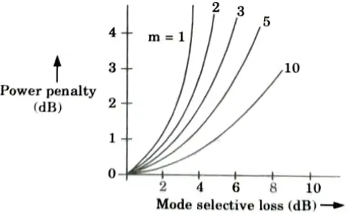
1. Interference between distinct propagating modes causes fluctuations in received power in multimode fibers. These variations are referred to as modal noise.
2. Fig. shows power penalty at
ii. Dispersive Pulse Broadening:
1. Group velocity dispersion reduces receiver sensitivity (GVD). By spreading the optical pulse, it restricts the bit rate distance product (BL).
2. Inter symbol interference exists as a result of pulse energy spreading.
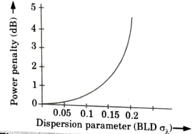
3. Several longitudinal modes change in multimode fiber while intensity remains constant. This results in mode partition noise (MPN).
4. It is claimed that a power penalty improves SNR in order to achieve the desired BER.
5. Fig. displays the power penalty at BER = 10-9 as a function of normalized dispersion parameter (BLD) for various mode partition coefficient values (K).
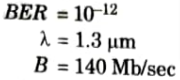
iii. Frequency Chirping:
1. Frequency chirping refers to the shift in carrier frequency caused by a change in refractive index.
2. Frequency chirp broadens the range of optical pulses, reducing system performance.
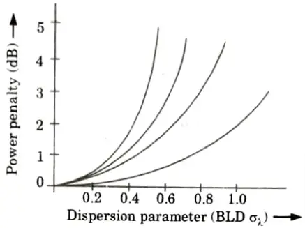
3. Fig. shows power penalty as a function of dispersion parameter BLD 𝛔𝛌 for several values of bit period.
iv. Reflection feedback and noise:
1. The light that reflects as a result of refractive index discontinuities at splices and connectors is unintended and may compromise receiver performance.
2. Reflection in fiber link originate at glass air interface, its reflectivity is given by
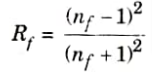
where, nf is refractive index of fiber material
3. The noise that results from random intensity fluctuation is called relative intensity noise (RIN). RIN is measured in dB/Hz.
6 thoughts on “Optical Communication: Aktu Notes and Solved Question Paper”